80C186EA/80C188EA AND 80L186EA/80L188EA 16-BIT HIGH-INTEGRATION EMBEDDED PROCESSORS Y Y Y Y Y 80C186 Upgrade for Power Critical Applications Fully Static Operation True CMOS Inputs and Outputs Integrated Feature Set Ð Static 186 CPU Core Ð Power Save, Idle and Powerdown Modes Ð Clock Generator Ð 2 Independent DMA Channels Ð 3 Programmable 16-Bit Timers Ð Dynamic RAM Refresh Control Unit Ð Programmable Memory and Peripheral Chip Select Logic Ð Programmable Wait State Generator Ð Local Bus Controller Ð Sys
80C186EA/80C188EA, 80L186EA/80L188EA 80C186EA/80C188EA AND 80L186EA/80L188EA 16-Bit High Integration Embedded Processor CONTENTS PAGE INTRODUCTION ÀÀÀÀÀÀÀÀÀÀÀÀÀÀÀÀÀÀÀÀÀÀÀÀÀÀÀ 4 80C186EA CORE ARCHITECTURE ÀÀÀÀÀÀÀ 4 Bus Interface Unit ÀÀÀÀÀÀÀÀÀÀÀÀÀÀÀÀÀÀÀÀÀÀÀÀÀÀ 4 Clock Generator ÀÀÀÀÀÀÀÀÀÀÀÀÀÀÀÀÀÀÀÀÀÀÀÀÀÀÀ 4 80C186EA PERIPHERAL ARCHITECTURE ÀÀÀÀÀÀÀÀÀÀÀÀÀÀÀÀÀÀÀÀÀÀÀÀ 5 Interrupt Control Unit ÀÀÀÀÀÀÀÀÀÀÀÀÀÀÀÀÀÀÀÀÀÀÀ 5 Timer/Counter Unit ÀÀÀÀÀÀÀÀÀÀÀÀÀÀÀÀÀÀÀÀÀÀÀÀ 5 DMA Control Unit ÀÀÀÀÀÀÀÀÀÀÀÀÀÀÀÀÀÀÀÀÀÀÀÀÀÀ 7
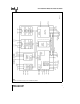
272432– 2 80C186EA/80C188EA, 80L186EA/80L188EA NOTE: Pin names in parentheses apply to the 80C186EA/80L188EA Figure 1.
80C186EA/80C188EA, 80L186EA/80L188EA INTRODUCTION Unless specifically noted, all references to the 80C186EA apply to the 80C188EA, 80L186EA, and 80L188EA. References to pins that differ between the 80C186EA/80L186EA and the 80C188EA/ 80L188EA are given in parentheses. The ‘‘L’’ in the part number denotes low voltage operation. Physically and functionally, the ‘‘C’’ and ‘‘L’’ devices are identical. The 80C186EA is the second product in a new generation of low-power, high-integration microprocessors.
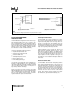
80C186EA/80C188EA, 80L186EA/80L188EA 272432 – 4 272432 – 3 (A) Crystal Connection (B) Clock Connection NOTE: The L1C1 network is only required when using a third-overtone crystal. Figure 2. Clock Configurations 80C186EA PERIPHERAL ARCHITECTURE The 80C186EA has integrated several common system peripherals with a CPU core to create a compact, yet powerful system. The integrated peripherals are designed to be flexible and provide logical interconnections between supporting units (e.g.
80C186EA/80C188EA, 80L186EA/80L188EA PCB Offset Function PCB Offset Function PCB Offset Function PCB Offset Function 00H Reserved 40H Reserved 80H Reserved C0H DMA0 Src. Lo 02H Reserved 42H Reserved 82H Reserved C2H DMA0 Src. Hi 04H Reserved 44H Reserved 84H Reserved C4H DMA0 Dest. Lo 06H Reserved 46H Reserved 86H Reserved C6H DMA0 Dest.
80C186EA/80C188EA, 80L186EA/80L188EA PCB Offset Function 20H Interrupt Vector 22H Specific EOI 24H Reserved 26H Reserved 28H Interrupt Mask 2AH Priority Mask 2C In-Service 2E Interrupt Request 30 Interrupt Status 32 TMR0 Interrupt Control 34 DMA0 Interrupt Control 36 DMA1 Interrupt Control 38 TMR1 Interrupt Control 3A TMR2 Interrupt Control 3C Reserved 3E Reserved Figure 4.
0C186EA/80C188EA, 80L186EA/80L188EA 80C187 Interface (80C186EA Only) The 80C187 Numerics Coprocessor may be used to extend the 80C186EA instruction set to include floating point and advanced integer instructions. Connecting the 80C186EA RESOUT and TEST/ BUSY pins to the 80C187 enables Numerics Mode operation. In Numerics Mode, three of the four MidRange Chip Select (MCS) pins become handshaking pins for the interface. The exchange of data and control information proceeds through four dedicated I/O ports.
80C186EA/80C188EA, 80L186EA/80L188EA PACKAGE INFORMATION This section describes the pins, pinouts, and thermal characteristics for the 80C186EA in the Plastic Leaded Chip Carrier (PLCC) package, Shrink Quad Flat Pack (SQFP), and Quad Flat Pack (QFP) package. For complete package specifications and information, see the Intel Packaging Outlines and Dimensions Guide (Order Number: 231369).
80C186EA/80C188EA, 80L186EA/80L188EA Table 2.
80C186EA/80C188EA, 80L186EA/80L188EA Table 3. Pin Descriptions Pin Name Pin Type Input Type Output States Description VCC P POWER connections consist of six pins which must be shorted externally to a VCC board plane. VSS G GROUND connections consist of five pins which must be shorted externally to a VSS board plane. CLKIN I OSCOUT O H(Q) R(Q) P(Q) OSCillator OUTput is only used when using a crystal to generate the external clock.
80C186EA/80C188EA, 80L186EA/80L188EA Table 3. Pin Descriptions (Continued) Pin Name Pin Type Input Type Output States A18:16 A19/S6–A16 (A19–A8) O H(Z) R(Z) P(X) These pins provide multiplexed Address during the address phase of the bus cycle. Address bits 16 through 19 are presented on these pins and can be latched using ALE. A18:16 are driven to a logic 0 during the data phase of the bus cycle. On the 8-bit bus versions, A15 – A8 provide valid address information for the entire bus cycle.
80C186EA/80C188EA, 80L186EA/80L188EA Table 3. Pin Descriptions (Continued) Pin Name Pin Type Input Type Output States WR/QS1 O ARDY I A(L) S(L) Asychronous ReaDY is an input to signal for the end of a bus cycle. ARDY is asynchronous on rising CLKOUT and synchronous on falling CLKOUT. ARDY or SRDY must be active to terminate any processor bus cycle, unless they are ignored due to correct programming of the Chip Select Unit.
80C186EA/80C188EA, 80L186EA/80L188EA Table 3. Pin Descriptions (Continued) Pin Name MCS0/PEREQ MCS1/ERROR MCS2 MCS3/NCS Pin Type Input Type Output States I/O A(L) H(1) R(1) P(1) These pins provide a multiplexed function. If enabled, these pins normally comprise a block of Mid-Range Chip Select outputs which will go active whenever the address of a memory bus cycle is within the address limitations programmed by the user.
80C186EA/80C188EA, 80L186EA/80L188EA 80C186EA PINOUT Tables 4 and 5 list the 80C186EA pin names with package location for the 68-pin Plastic Leaded Chip Carrier (PLCC) component. Figure 9 depicts the complete 80C186EA/80L186EA pinout (PLCC package) as viewed from the top side of the component (i.e., contacts facing down). Tables 6 and 7 list the 80C186EA pin names with package location for the 80-pin Quad Flat Pack (EIAJ) component.
80C186EA/80C188EA, 80L186EA/80L188EA Table 5.
80C186EA/80C188EA, 80L186EA/80L188EA Table 6.
80C186EA/80C188EA, 80L186EA/80L188EA Table 7. QFP (EIAJ) Package Location with Pin Names Location Name Location Name Location Name Location Name 1 2 3 4 5 6 7 8 9 10 11 12 13 14 15 16 17 18 19 20 AD15 (A15) VCC A16 A17 A18 A19/S6 BHE (RFSH) WR/QS1 RD/QSMD ALE/QS0 N.C. VSS VSS N.C. N.C.
80C186EA/80C188EA, 80L186EA/80L188EA Table 8. SQFP Pin Functions with Package Location AD Bus AD0 AD1 AD2 AD3 AD4 AD5 AD6 AD7 AD8 (A8) AD9 (A9) AD10 (A10) AD11 (A11) AD12 (A12) AD13 (A13) AD14 (A14) AD15 (A15) A16/S3 A17/S4 A18/S5 A19/S6 Bus Control 1 3 6 8 12 14 16 18 2 5 7 9 13 15 17 19 21 22 23 24 29 26 40 39 38 28 27 37 44 56 54 45 43 42 No Connection N.C. N.C. N.C. N.C.
80C186EA/80C188EA, 80L186EA/80L188EA 272432 – 7 Figure 7. Shrink Quad Flat Pack (SQFP) Pinout Diagram NOTES: 1. XXXXXXXXD indicates the Intel FPO number. 2. Pin names in parentheses apply to the 80C188EA.
80C186EA/80C188EA, 80L186EA/80L188EA ELECTRICAL SPECIFICATIONS Absolute Maximum Ratings* Storage Temperature ÀÀÀÀÀÀÀÀÀÀ b 65§ C to a 150§ C Case Temperature under Bias ÀÀÀ b 65§ C to a 150§ C Supply Voltage with Respect to VSS ÀÀÀÀÀÀÀÀÀÀÀÀÀÀÀÀÀÀÀÀÀÀÀ b 0.5V to a 6.5V Voltage on Other Pins with Respect to VSS ÀÀÀÀÀÀÀÀÀÀÀÀÀÀÀÀÀÀ b 0.5V to VCC a 0.5V Recommended Connections Power and ground connections must be made to multiple VCC and VSS pins.
80C186EA/80C188EA, 80L186EA/80L188EA DC SPECIFICATIONS (80C186EA/80C188EA) Symbol Parameter Min Max Units Conditions VCC Supply Voltage 4.5 5.5 V VIL Input Low Voltage for All Pins b 0.5 0.3 VCC V VIH Input High Voltage for All Pins 0.7 VCC VCC a 0.5 V VOL Output Low Voltage 0.45 V IOL e 3 mA (min) VOH Output High Voltage VCC b 0.5 V IOH e b 2 mA (min) VHYR Input Hysterisis on RESIN 0.
80C186EA/80C188EA, 80L186EA/80L188EA DC SPECIFICATIONS (80L186EA/80L188EA) Symbol Parameter Min Max Units Conditions VCC Supply Voltage 2.7 5.5 V VIL Input Low Voltage for All Pins b 0.5 0.3 VCC V VIH Input High Voltage for All Pins 0.7 VCC VCC a 0.5 V VOL Output Low Voltage 0.45 V IOL e 1.6 mA (min) VOH Output High Voltage VCC b 0.5 V IOH e b 1 mA (min) VHYR Input Hysterisis on RESIN 0.
80C186EA/80C188EA, 80L186EA/80L188EA ICC VERSUS FREQUENCY AND VOLTAGE PDTMR PIN DELAY CALCULATION The current (ICC) consumption of the processor is essentially composed of two components; IPD and ICCS. The PDTMR pin provides a delay between the assertion of NMI and the enabling of the internal clocks when exiting Powerdown. A delay is required only when using the on-chip oscillator to allow the crystal or resonator circuit time to stabilize.
80C186EA/80C188EA, 80L186EA/80L188EA AC SPECIFICATIONS AC CharacteristicsÐ80C186EA25/80C186EA20/80C186EA13 Symbol Parameter INPUT CLOCK TF TC TCH TCL TCR TCF CLKIN Frequency CLKIN Period CLKIN High Time CLKIN Low Time CLKIN Rise Time CLKIN Fall Time Min Max 25 MHz(12) Min Max 20 MHz Min Max Units Notes 13 MHz 0 20 10 10 1 1 50 % % % 8 8 0 25 10 10 1 1 40 % % % 8 8 0 38.
80C186EA/80C188EA, 80L186EA/80L188EA AC SPECIFICATIONS (Continued) AC CharacteristicsÐ80C186EA25/80C186EA20/80C186EA13 Symbol Parameter SYNCHRONOUS INPUTS Min Max 25 MHz(12) Min Max 20 MHz Min Max Units Notes 13 MHz TCHIS TEST, NMI, INT3:0, T1:0IN, ARDY 8 10 10 ns 1, 9 TCHIH TEST, NMI, INT3:0, T1:0IN, ARDY 3 3 3 ns 1, 9 TCLIS AD15:0 (AD7:0), ARDY, SRDY, DRQ1:0 10 10 10 ns 1, 10 TCLIH AD15:0 (AD7:0), ARDY, SRDY, DRQ1:0 3 3 3 ns 1, 10 TCLIS HOLD, PEREQ, ERROR (80C18
80C186EA/80C188EA, 80L186EA/80L188EA AC SPECIFICATIONS AC CharacteristicsÐ80L186EA13/80L186EA8 Symbol Parameter Min INPUT CLOCK TF TC TCH TCL TCR TCF CLKIN Frequency CLKIN Period CLKIN High Time CLKIN Low Time CLKIN Rise Time CLKIN Fall Time Max Min 13 MHz Max Units Notes 8 MHz 0 38.5 12 12 1 1 26 % % % 8 8 0 62.
80C186EA/80C188EA, 80L186EA/80L188EA AC SPECIFICATIONS AC CharacteristicsÐ80L186EA13/80L186EA8 Symbol Parameter SYNCHRONOUS INPUTS Min Max Min Units Notes 22 ns 1, 9 13 MHz 22 Max 8 MHz TCHIS TEST, NMI, INT3:0, T1:0IN, ARDY TCHIH TEST, NMI, INT3:0, T1:0IN, ARDY 3 3 ns 1, 9 TCLIS AD15:0 (AD7:0), ARDY, SRDY, DRQ1:0 22 22 ns 1, 10 TCLIH AD15:0 (AD7:0), ARDY, SRDY, DRQ1:0 3 3 ns 1, 10 TCLIS HOLD 22 22 ns 1, 9 TCLIH HOLD 3 3 ns 1, 9 TCLIS RESIN (to CLKIN) 22 22
80C186EA/80C188EA, 80L186EA/80L188EA AC SPECIFICATIONS (Continued) Relative Timings (80C186EA25/20/13, 80L186EA13/8) Symbol Parameter Min Max Unit Notes RELATIVE TIMINGS TLHLL ALE Rising to ALE Falling T b 15 ns TAVLL TPLLL Address Valid to ALE Falling (/2T b 10 ns Chip Selects Valid to ALE Falling (/2T b 10 ns TLLAX Address Hold from ALE Falling (/2T b 10 ns TLLWL ALE Falling to WR Falling (/2T b 15 ns 1 TLLRL ALE Falling to RD Falling (/2T b 15 ns 1 TRHLH RD Rising to ALE
80C186EA/80C188EA, 80L186EA/80L188EA AC TEST CONDITIONS The AC specifications are tested with the 50 pF load shown in Figure 8. See the Derating Curves section to see how timings vary with load capacitance. 272432 – 8 CL e 50 pF for all signals. Specifications are measured at the VCC/2 crossing point, unless otherwise specified. See AC Timing Waveforms, for AC specification definitions, test pins, and illustrations. Figure 8. AC Test Load AC TIMING WAVEFORMS 272432 – 9 Figure 9.
80C186EA/80C188EA, 80L186EA/80L188EA 272432 – 10 NOTE: 20% VCC k Float k 80% VCC Figure 10. Output Delay and Float Waveform 272432 – 11 NOTE: RESIN measured to CLKIN, not CLKOUT Figure 11.
80C186EA/80C188EA, 80L186EA/80L188EA 272432 – 12 NOTES: 1. TDXDL for write cycle followed by read cycle. 2. Pin names in parentheses apply to tthe 80C188EA. Figure 12.
80C186EA/80C188EA, 80L186EA/80L188EA DERATING CURVES 272432 – 13 Figure 13. Typical Output Delay Variations Versus Load Capacitance RESET The processor performs a reset operation any time the RESIN pin is active. The RESIN pin is actually synchronized before it is presented internally, which means that the clock must be operating before a reset can take effect. From a power-on state, RESIN must be held active (low) in order to guarantee correct initialization of the processor.
NOTES: 1. CLKOUT synchronization occurs approximately 1(/2 CLKIN periods after RESIN is sampled low. 2. Pin names in parentheses apply to the 80C188EA. 272432– 15 80C186EA/80C188EA, 80L186EA/80L188EA Figure 15.
NOTES: 1. CLKOUT resynchronization occurs approximately 1(/2 CLKIN periods after RESIN is sampled low. If RESIN is sampled low while CLKOUT is transitioning high, then CLKOUT will remain high for two CLKIN periods. If RESIN is sampled low while CLKOUT is transitioning high, then CLKOUT will not be affected. 2. Pin names in parentheses apply to the 80C188EA. 272432– 16 80C186EA/80C188EA, 80L186EA/80L188EA Figure 16.
80C186EA/80C188EA, 80L186EA/80L188EA BUS CYCLE WAVEFORMS Figures 17 through 23 present the various bus cycles that are generated by the processor. What is shown in the figure is the relationship of the various bus signals to CLKOUT. These figures along with the information present in AC Specifications allow the user to determine all the critical timing analysis needed for a given application. 272432-17 NOTES: 1. During the data phase of the bus cycle, A19/S6 is driven high for a DMA or refresh cycle. 2.
80C186EA/80C188EA, 80L186EA/80L188EA 272432-18 NOTES: 1. During the data phase of the bus cycle, A19/S6 is driven high for a DMA cycle. 2. Pin names in parentheses apply to the 80C188EA. Figure 18.
80C186EA/80C188EA, 80L186EA/80L188EA 272432 – 19 NOTES: 1. The processor drives these pins to 0 during Idle and Powerdown Modes. 2. Pin names in parentheses apply to the 80C188EA. Figure 19.
80C186EA/80C188EA, 80L186EA/80L188EA NOTES: 1. INTA occurs one clock later in Slave Mode. 2. Pin names in parentheses apply to the 80C188EA. 272432 – 20 Figure 20.
80C186EA/80C188EA, 80L186EA/80L188EA 272432 – 21 NOTE: 1. Pin names in parentheses apply to the 80C188EA. Figure 21.
80C186EA/80C188EA, 80L186EA/80L188EA 272432 – 22 NOTE: 1. Pin names in parentheses apply to the 80C188EA. Figure 22.
80C186EA/80C188EA, 80L186EA/80L188EA 272432 – 23 NOTES: 1. Generalized diagram for READ or WRITE. 2. ARDY low by either edge causes a wait state. Only rising ARDY is fully synchronized. 3. SRDY low causes a wait state. SRDY must meet setup and hold times to ensure correct device operation. 4. Either ARDY or SRDY active high will terminate a bus cycle. 5. Pin names in parentheses apply to the 80C188EA. Figure 23.
80C186EA/80C188EA, 80L186EA/80L188EA 80C186EA/80C188EA EXECUTION TIMINGS A determination of program exeuction timing must consider the bus cycles necessary to prefetch instructions as well as the number of execution unit cycles necessary to execute instructions. The following instruction timings represent the minimum execution time in clock cycle for each instruction.
80C186EA/80C188EA, 80L186EA/80L188EA INSTRUCTION SET SUMMARY Function Format 80C186EA Clock Cycles 80C188EA Clock Cycles 2/12* Comments DATA TRANSFER MOV e Move: Register to Register/Memory 1000100w mod reg r/m 2/12 Register/memory to register 1000101w mod reg r/m 2/9 2/9 Immediate to register/memory 1100011w mod 000 r/m data 12–13 12–13 8/16-bit 8/16-bit data if w e 1 Immediate to register 1 0 1 1 w reg data data if w e 1 3–4 3–4 Memory to accumulator 1010000w addr-low addr
80C186EA/80C188EA, 80L186EA/80L188EA INSTRUCTION SET SUMMARY (Continued) Function Format 80C186EA Clock Cycles 80C188EA Clock Cycles Comments DATA TRANSFER (Continued) SEGMENT e Segment Override: CS 00101110 2 2 SS 00110110 2 2 DS 00111110 2 2 ES 00100110 2 2 3/10 3/10* 4/16 4/16* 3/4 3/4 3/10 3/10* 4/16 4/16* 3/4 3/4 3/15 3/15* 3 3 3/10 3/10* 4/16 4/16* 3/4 3/4 3/10 3/10* 4/16 4/16* 3/4 3/4* 3/15 3/15* 3 3 ARITHMETIC ADD e Add: Reg/memory with register
80C186EA/80C188EA, 80L186EA/80L188EA INSTRUCTION SET SUMMARY (Continued) Function Format 80C186EA Clock Cycles 80C188EA Clock Cycles 25–28 34–37 31–34 40–43 25–28 34–37 32–34 40–43* 22–25 29–32 22-25 29–32 29 38 35 44 29 38 35 44* 44–52 53–61 50–58 59–67 44–52 53–61 50–58 59–67* Comments ARITHMETIC (Continued) IMUL e Integer multiply (signed): 1111011w mod 1 0 1 r/m Register-Byte Register-Word Memory-Byte Memory-Word IMUL e Integer Immediate multiply (signed) 011010s1 mod reg r/m DIV e D
80C186EA/80C188EA, 80L186EA/80L188EA INSTRUCTION SET SUMMARY (Continued) Function Format 80C186EA Clock Cycles 80C188EA Clock Cycles 3/10 3/10* 4/16 4/16* 3/4 3/4 3/10 3/10* Comments LOGIC (Continued) XOR e Exclusive or: Reg/memory and register to either 001100dw mod reg r/m Immediate to register/memory 1000000w mod 1 1 0 r/m data Immediate to accumulator 0011010w data data if w e 1 NOT e Invert register/memory 1111011w mod 0 1 0 r/m data if w e 1 8/16-bit STRING MANIPULATION M
80C186EA/80C188EA, 80L186EA/80L188EA INSTRUCTION SET SUMMARY (Continued) Function Format 80C186EA Clock Cycles 80C188EA Clock Cycles 16 20 Comments CONTROL TRANSFER (Continued) RET e Return from CALL: Within segment 11000011 Within seg adding immed to SP 11000010 Intersegment 11001011 Intersegment adding immediate to SP 11001010 data-low 25 33 JE/JZ e Jump on equal/zero 01110100 disp 4/13 4/13 JL/JNGE e Jump on less/not greater or equal 01111100 disp 4/13 4/13 JLE/JNG e Jump on
80C186EA/80C188EA, 80L186EA/80L188EA INSTRUCTION SET SUMMARY (Continued) Function Format 80C186EA Clock Cycles 80C188EA Clock Cycles 2 2 Comments PROCESSOR CONTROL CLC e Clear carry 11111000 CMC e Complement carry 11110101 2 2 STC e Set carry 11111001 2 2 CLD e Clear direction 11111100 2 2 STD e Set direction 11111101 2 2 CLI e Clear interrupt 11111010 2 2 STI e Set interrupt 11111011 2 2 HLT e Halt 11110100 2 2 WAIT e Wait 10011011 6 6 LOCK e Bus lock prefix 11110
80C186EA/80C188EA, 80L186EA/80L188EA REVISION HISTORY ERRATA Intel 80C186EA/80L186EA devices are marked with a 9-character alphanumeric Intel FPO number underneath the product number. This data sheet update is valid for devices with an ‘‘A’’, ‘‘B’’, ‘‘C’’, ‘‘D’’, or ‘‘E’’ as the ninth character in the FPO number, as illustrated in Figure 5 for the 68-lead PLCC package, Figure 6 for the 84-lead QFP (EIAJ) package, and Figure 7 for the 80-lead SQFP device.