
32-Bit High-Performance Superscalar Processor Data Sheet
80960HA/HD/HT
44 Datasheet
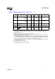
Table 24. A.C. Characteristics Notes
NOTES:
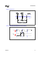
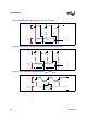
1. See Section 4.8, “AC Timing Waveforms” on page 46 for waveforms and definitions.
2. See
Figure 25, “Output Delay or Hold vs. Load Capacitance” on page 52 for capacitive derating information
for output delays and hold times.
3. See Figure 22, “Rise and Fall Time Derating at 85 ° C and Minimum VCC” on page 51 for capacitive
derating information for rise and fall times.
4. Where N is the number of N
RAD
, N
RDD
, N
WAD
or N
WDD
wait states that are programmed in the Bus
Controller Region Table. WAIT
never goes active when there are no wait states in an access.
5. N = Number of wait states inserted with READY.
6. These specifications are ensured by the processor.
7. These specifications must be met by the system for proper operation of the processor.
8. RESET
is an asynchronous input that has no required setup and hold time for proper operation. However,
to ensure the device exits the reset mode synchronized to a particular clock edge, the rising edge of
RESET must meet setup and hold times to the rising edge of the CLKIN.
9. The interrupt pins are synchronized internally by the 80960Hx. They have no required setup or hold times
for proper operation. These pins are sampled by the interrupt controller every clock and must be active for
at least two consecutive CLKIN rising edges when asserting them asynchronously. To ensure recognition at
a particular clock edge, the setup and hold times shown must be met.
10.Relative Output timings are not tested.
11.Not tested.
12.The processor minimizes changes to the bus signals when transitioning from a bus cycle to an idle bus for
the following signals: A31:4, SUP
, CT3:0, D/C, LOCK, W/R, BE3:0.
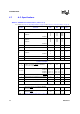
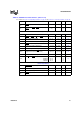
Table 25. 80960Hx Boundary Scan Test Signal Timings
Symbol Parameter Min Max Units Notes
T
BSF
TCK Frequency 0 8 MHz
T
BSC
TCK Period 125 Infinite ns
T
BSCH
TCK High Time 40 ns Measured at 1.5 V
†
T
BSCL
TCK Low Time 40 ns Measured at 1.5 V
†
T
BSCR
TCK Rise Time 8 ns 0.8 V to 2.0 V
†
T
BSCF
TCK Fall Time 8 ns 2.0 V to 0.8 V
†
T
BSIS1
Input Setup to TCK —
TDI, TMS
8ns
T
BSIH1
Input Hold from TCK —
TDI, TMS
10 ns
T
BSOV1
TDO Valid Delay 3 30 ns
T
BSOF1
TDO Float Delay 36 ns
†
T
BSOV2
All Outputs (Non-Test)
Valid Delay
330ns
Relative to TCK
T
BSOF2
All Outputs (Non-Test)
Float Delay
36 ns
Relative to TCK
†
T
BSIS2
Input Setup to TCK - All
Inputs (Non-Test)
8ns
T
BSIH2
Input Hold from TCK - All
Inputs (Non-Test)
10 ns
† Not tested.