80960HA/HD/HT 32-Bit High-Performance Superscalar Processor Datasheet Product Features ■ ■ ■ ■ ■ ■ 32-Bit Parallel Architecture — Load/Store Architecture — Sixteen 32-Bit Global Registers — Sixteen 32-Bit Local Registers — 1.
INFORMATION IN THIS DOCUMENT IS PROVIDED IN CONNECTION WITH INTEL® PRODUCTS. NO LICENSE, EXPRESS OR IMPLIED, BY ESTOPPEL OR OTHERWISE, TO ANY INTELLECTUAL PROPERTY RIGHTS IS GRANTED BY THIS DOCUMENT.
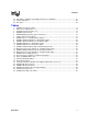
Contents Contents 1.0 About This Document ................................................................................................................... 9 2.0 Intel 80960Hx Processor ............................................................................................................... 9 2.1 2.2 2.3 3.0 The i960® Processor Family ...............................................................................................10 Key 80960Hx Features ..........................................
Contents 7 8 9 10 11 12 13 14 15 16 17 18 19 20 21 22 23 24 25 26 27 28 29 30 31 32 33 34 35 36 37 38 39 40 41 42 43 44 45 46 47 48 49 50 51 52 53 54 55 56 4 VCC5 Current-Limiting Resistor ................................................................................................. 38 AC Test Load.............................................................................................................................. 45 CLKIN Waveform...............................................................
Contents 57 A Summary of Aligned and Unaligned Transfers for 8-Bit Bus...................................................81 58 Idle Bus Operation ......................................................................................................................82 59 Bus States ..................................................................................................................................
Contents Revision History Date Revision History Formatted the datasheet in a new template. In “32-Bit Parallel Architecture” on page 1: • Removed operating frequency of 16/32 (bus/core) from 80960HD. • Removed operating frequency of 20/60 (bus/core) from 80960HT. In Table 5 “80960HA/HD/HT Package Types and Speeds” on page 14: September 2002 008 • Removed core speed of 32 MHz and bus speed of 16 MHz, and order number A80960HD32-S-L2GG from the 168L PGA package, 80960HD device.
Contents Date Revision History In Table 23 “80960Hx AC Characteristics” on page 42: • Added overbars where required. • Modified TDVNH to list separate specifications for 3.3 V and 5 V. July 1998 (continued) 007 (continued) • Modified TOV2, TOH2 and TTVEL to reflect specific 80960HA, 80960HD and 80960HT values. In Figure 23 “ICC Active (Power Supply) vs. Frequency” on page 51: • Changed ‘5’ to ‘0’ on the CLKIN Frequency axis.
Contents This page intentionally left blank.
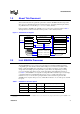
80960HA/HD/HT 1.0 About This Document This document describes the parametric performance of Intel’s 80960Hx embedded superscalar microprocessors. Detailed descriptions for functional topics, other than parametric performance, are published in the i960® Hx Microprocessor User’s Guide (272484). In this document, ‘80960Hx’ and ‘i960 Hx processor’ refer to the products described in Table 1. Throughout this document, information that is specific to each is clearly indicated. Figure 1.
80960HA/HD/HT In addition to expanded clock frequency options, the 80960Hx provides essential enhancements for an emerging class of high-performance embedded applications. Features include a larger instruction cache, data cache, and data RAM than any other 80960 processor to date. It also boasts a 32-bit demultiplexed and pipelined burst bus, fast interrupt mechanism, guarded memory unit, wait state generator, dual programmable timers, ONCE and IEEE 1149.
80960HA/HD/HT subsystems with minimum system complexity. To reduce the effect of wait states, the bus design is decoupled from the core. This lets the processor execute instructions while the bus performs memory accesses independently. The Bus Controller’s key features include: • • • • • • • • 2.2.
80960HA/HD/HT 2.2.6 Dual Programmable Timers The processor provides two independent 32-bit timers, with four programmable clock rates. The user configures the timers through the Timer Unit registers. These registers are memory-mapped within the 80960Hx, addressable on 32-bit boundaries. The timers have a single-shot mode and auto-reload capabilities for continuous operation. Each timer has an independent interrupt request to the processor’s interrupt controller. 2.2.
80960HA/HD/HT 2.3 Instruction Set Summary Table 4 summarizes the 80960Hx instruction set by logical groupings. Table 4.
80960HA/HD/HT 3.0 Package Information This section describes the pins, pinouts and thermal characteristics for the 80960Hx in the 168-pin ceramic Pin Grid Array (PGA) package, 208-pin PowerQuad2* (PQ4). For complete package specifications and information, see the Intel Packaging Handbook (Order# 240800). The 80960HA/HD/HT is offered with eight speeds and two package types (Table 5).
80960HA/HD/HT 3.1 Pin Descriptions This section defines the 80960Hx pins. Table 6 presents the legend for interpreting the pin descriptions in Table 7. All pins float while the processor is in the ONCE mode, except TDO, which may be driven active according to normal JTAG specifications. Table 6. Pin Description Nomenclature Symbol I Input only pin. O Output only pin. I/O Pin may be input or output. - Datasheet Description Pin must be connected as indicated for proper device functionality.
80960HA/HD/HT Table 7. 80960Hx Processor Family Pin Descriptions (Sheet 1 of 4) Name Type Description O A31:2 H(Z) B(Z) R(Z) ADDRESS BUS carries the upper 30 bits of the physical address. A31 is the most significant address bit and A2 is the least significant. During a bus access, A31:2 identify all external addresses to word (4-byte) boundaries. The byte enable signals indicate the selected byte in each word. During burst accesses, A3 and A2 increment to indicate successive addresses.
80960HA/HD/HT Table 7. 80960Hx Processor Family Pin Descriptions (Sheet 2 of 4) Name Type O SUP H(Z) B(Z) R(1) Description SUPERVISOR ACCESS indicates whether the current bus access originates from a request issued while in supervisor mode or user mode. SUP may be used by the memory subsystem to isolate supervisor code and data structures from non-supervisor access.
80960HA/HD/HT Table 7. 80960Hx Processor Family Pin Descriptions (Sheet 3 of 4) Name Type Description HOLD REQUEST signals that an external agent requests access to the processor’s address, data, and control buses. When HOLD is asserted, the processor: HOLD I S(L) Completes the current bus request. Asserts HOLDA and floats the address, data, and control buses. When HOLD is deasserted, the HOLDA pin is deasserted and the processor reassumes control of the address, data, and control pins.
80960HA/HD/HT Table 7. 80960Hx Processor Family Pin Descriptions (Sheet 4 of 4) Name CLKIN RESET STEST Type I I A(L) I S(L) O FAIL H(Q) B(Q) R(0) Description CLOCK INPUT provides the time base for the 80960Hx. All internal circuitry is synchronized to CLKIN. All input and output timings are specified relative to CLKIN. For the 80960HD, the 2x internal clock is derived by multiplying the CLKIN frequency by two.
80960HA/HD/HT 3.2 80960Hx Mechanical Data 3.2.1 80960Hx PGA Pinout Figure 2 depicts the complete 80960Hx PGA pinout as viewed from the top side of the component (i.e., pins facing down). Figure 3 shows the complete 80960Hx PGA pinout as viewed from the pin-side of the package (i.e., pins facing up). Table 9 lists the 80960Hx pin names with package location. See Section 4.3, “Recommended Connections” on page 38 for specifications and recommended connections. Figure 2.
80960HA/HD/HT Figure 3.
80960HA/HD/HT Table 8.
80960HA/HD/HT Table 8.
80960HA/HD/HT Table 9.
80960HA/HD/HT Table 9.
80960HA/HD/HT 3.2.2 80960Hx PQ4 Pinout Figure 4.
80960HA/HD/HT Table 10.
80960HA/HD/HT Table 10.
80960HA/HD/HT Table 11.
80960HA/HD/HT Table 11.
80960HA/HD/HT 3.3 Package Thermal Specifications The 80960Hx is specified for operation when TC (case temperature) is within the range of 0 °C to 85 °C. TC may be measured in any environment to determine whether the 80960Hx is within the specified operating range. Measure the case temperature at the center of the top surface, opposite the pins. Refer to Figure 5. TA (ambient temperature) is calculated from θCA (thermal resistance from case to ambient) using Equation 1: Equation 1.
80960HA/HD/HT Table 12. Maximum TA at Various Airflows in °C (PGA Package Only) Airflow-ft/min (m/sec) Core 1X Bus Clock Core 2X Bus Clock Core 3X Bus Clock fCLKIN (MHz) 0 (0) 200 (1.01) 400 (2.03) 600 (3.04) 800 (4.06) 1000 (5.
80960HA/HD/HT Table 14. Maximum TA at Various Airflows in °C (PQ4 Package Only) Airflow-ft/min (m/sec) Core 1X Bus Clock Core 2X Bus Clock Core 3X Bus Clock fCLKIN (MHz) 0 (0) 200 (1.01) 400 (2.03) 600 (3.04) 800 (4.06) 1000 (5.
80960HA/HD/HT 3.4 Heat Sink Adhesives Intel recommends silicone-based adhesives to attach heat sinks to the PGA package. There is no particular recommendation concerning the PQ4 package. 3.5 PowerQuad4 Plastic Package The 80960Hx family is available in an improved version of the common 208-lead SQFP plastic package called the PowerQuad4* (PQ4). The PQ4 package dimensions and lead pitch are identical to the SQFP package and the former PQ2 package, so the PQ4 fits into the same board footprint.
80960HA/HD/HT Table 16. Fields of 80960Hx Device ID Field Value Definition Version See Table 18. Indicates major stepping changes. VCC 1 = 3.3 V device Indicates that a device is 3.3 V. Product Type 00 0100 (Indicates i960 CPU) Designates type of product. Generation Type 0010 = H-series Indicates the generation (or series) the product belongs to. Model See Table 17. Indicates member within a series and specific model information.
80960HA/HD/HT 3.7 Sources for Accessories The following is a list of suggested sources for 80960Hx accessories. This is neither an endorsement nor a warranty of the performance of any of the listed products and/or companies. Sockets • 3M Textool Test and Interconnection Products 6801 River Place Blvd. MS 130-3N-29 Austin, TX 78726-9000 (800) 328-0411 FAX: (800) 932-9373 • Concept Mfg, Inc. (Decoupling Sockets) 400 Walnut St.
80960HA/HD/HT 4.0 Electrical Specifications 4.1 Absolute Maximum Ratings Table 19. Absolute Maximum Ratings Warning: 4.2 Parameter Maximum Rating Storage Temperature –65 ºC to +150 ºC Case Temperature Under Bias –65 ºC to +110 ºC Supply Voltage with respect to VSS –0.5 V to + 4.6 V Voltage on VCC5 with respect to VSS –0.5 V to + 6.5 V Voltage on Other Pins with respect to VSS –0.5 V to VCC5 + 0.5 V Stressing the device beyond the “Absolute Maximum Ratings” may cause permanent damage.
80960HA/HD/HT 4.3 Recommended Connections Power and ground connections must be made to multiple VCC and VSS (GND) pins. Every 80960Hx-based circuit board should include power (VCC) and ground (VSS) planes for power distribution. Every VCC pin must be connected to the power plane; every VSS pin must be connected to the ground plane. Pins identified as “NC” —no connect pins—must not be connected in the system. Liberal decoupling capacitance should be placed near the 80960Hx.
80960HA/HD/HT Table 21. VDIFF Specification for Dual Power Supply Requirements (3.3 V, 5 V) Sym VDIFF 4.5 Parameter VCC5-VCC Difference Min Max Units Notes 2.25 V VCC5 input should not exceed VCC by more than 2.25 V during power-up and power-down, or during steady-state operation. VCCPLL Pin Requirements When the voltage on the VCCPLL power supply pin exceeds the VCC pin voltage by 0.
80960HA/HD/HT 4.6 D.C.Specifications Table 22. 80960Hx D.C. Characteristics (Sheet 1 of 2) Per the conditions described in Section 4.3, “Recommended Connections” on page 38. Symbol Parameter Min Typ Max Units Notes VIL Input Low Voltage – 0.3 +0.8 V VIH Input High Voltage 2.0 VCC5 + 0.3 V All outputs except FAIL 0.4 0.2 V IOL = 3 mA IOL = 100 µA VOL Output Low Voltage FAIL pin 0.4 V IOL = 5 mA VOH Output High Voltage V V IOH = –3 mA IOH = –100 µA VOL Output Low Voltage 2.
80960HA/HD/HT Table 22. 80960Hx D.C. Characteristics (Sheet 2 of 2) Per the conditions described in Section 4.3, “Recommended Connections” on page 38.
80960HA/HD/HT 4.7 A.C. Specifications Table 23. 80960Hx A.C. Characteristics (Sheet 1 of 2) Per conditions in Section 4.2, “Operating Conditions” on page 37 and Section 4.7.1, “AC Test Conditions” on page 45. Symbol Parameter Min Max Units Notes 16 16 16 40 40 25 MHz MHz MHz 25 25 40 62.5 62.5 62.
80960HA/HD/HT Table 23. 80960Hx A.C. Characteristics (Sheet 2 of 2) Per conditions in Section 4.2, “Operating Conditions” on page 37 and Section 4.7.1, “AC Test Conditions” on page 45. Symbol TIS2 TIH2 Parameter Min Input Setup for READY, BTERM, HOLD, and BOFF Input Hold for READY, BTERM, HOLD, and BOFF Max Units 6 ns 2.
80960HA/HD/HT Table 24. A.C. Characteristics Notes NOTES: 1. See Section 4.8, “AC Timing Waveforms” on page 46 for waveforms and definitions. 2. See Figure 25, “Output Delay or Hold vs. Load Capacitance” on page 52 for capacitive derating information for output delays and hold times. 3. See Figure 22, “Rise and Fall Time Derating at 85 °C and Minimum VCC” on page 51 for capacitive derating information for rise and fall times. 4.
80960HA/HD/HT 4.7.1 A.C. Test Conditions A.C. values are derived using the 50 pF load shown in Figure 8. Figure 25, “Output Delay or Hold vs. Load Capacitance” on page 52, shows how timings vary with load capacitance. Input waveforms (except for CLKIN) are assumed to have a rise and fall time of ≤ 2 ns from 0.8 V to 2.0 V. Figure 8. A.C.
80960HA/HD/HT 4.8 A.C. Timing Waveforms Figure 9. CLKIN Waveform TCR TCF 2.0 V 1.5 V 0.8 V TCH TCL T Figure 10. Output Delay Waveform 1.5 V CLKIN Outputs: A31:2, D31:0 write only, DP3:0 write only PCHK, BE3:0, W/R, D/C, SUP, ADS, DEN, LOCK, HOLDA, BREQ, BSTALL, CT3:0, FAIL, WAIT, BLAST TOH1 1.5 V TOV1 Max Min 1.5 V 1.5 V Figure 11. Output Delay Waveform CLKIN 1.5 V 1.5 V TOV2 TOH2 DT/R 46 1.5 V Min Max 1.
80960HA/HD/HT Figure 12. Output Float Waveform 1.5 V CLKIN Outputs: A31:2, D31:0 write only, DP3:0 write only PCHK, BE3:0, W/R, D/C, SUP, ADS, DEN, LOCK, HOLDA, TOF 1.5 V Max Min CT3:0, WAIT, BLAST, DT/R Figure 13. Input Setup and Hold Waveform 1.5 V CLKIN 1.5 V 1.5 V TIH TIS Min Min Inputs: READY, HOLD, BTERM, BOFF, D31:0 on reads, DP3:0 on reads, RESET Valid Figure 14. NMI, XINT7:0 Input Setup and Hold Waveform A CLKIN B 1.5 V A 1.
80960HA/HD/HT Figure 15. Hold Acknowledge Timings CLKIN HOLD 1.5 V TIH TIS Min Min 1.5 V TIH TIS Min Min 1.5 V 1.5 V TOV1 TOH1 HOLDA 1.5 V 1.5 V TOV1 Max Min 1.5 V TOH1 Max Min 1.5 V 1.5 V TOV TOH — OUTPUT DELAY - The maximum output delay is referred to as the Output Valid Delay (TOV). The minimum output delay is referred to as the Output Hold (TOH).
80960HA/HD/HT Figure 17. TCK Waveform TBSCR TBSCF 2.0 V 1.5 V 0.8 V TBSCH TBSCL TBSC Figure 18. Input Setup and Hold Waveforms for TBSIS1 and TBSIH1 TCLK 1.5 V 1.5 V TBSIS1 Inputs: TMS TDI Datasheet 1.5 V 1.5 V TBSIH1 Valid 1.
80960HA/HD/HT Figure 19. Output Delay and Output Float for TBSOV1 and TBSOF1 TCK 1.5 V 1.5 V TBSOV1 TDO 1.5 V TBSOF1 Valid 1.5 V Figure 20. Output Delay and Output Float Waveform for TBSOV2 and TBSOF2 TCK 1.5 V 1.5 V TBSOV2 Non-Test Outputs 1.5 V 1.5 V TBSOF2 Valid Figure 21. Input Setup and Hold Waveform for TBSIS2 and TBSIH2 TCK 1.5 V 1.5 V 1.5 V TBSIS2 TBSIH2 Non-Test Inputs 50 1.5 V Valid 1.
80960HA/HD/HT Figure 22. Rise and Fall Time Derating at 85 °C and Minimum VCC 5 Time (ns) 4 3 2.0 to 0.8 V 0.8 to 2.0 V 2 1 50pF 100pF 150pF CL (pF) Figure 23. ICC Active (Power Supply) vs.
80960HA/HD/HT Figure 24. ICC Active (Thermal) vs. Frequency 1400 ICC Active (Thermal) (mA) 1200 1000 800 HA 600 HD 400 HT 200 10 20 30 40 CLKIN Frequency (MHz) Output Valid Delays (ns) @ 1.5 V Figure 25. Output Delay or Hold vs. Load Capacitance nom + 10 5.5 V Input Signals 3.
80960HA/HD/HT Figure 26. Output Delay vs. Temperature Output Valid Delays (ns) @ 1.5 V Processor Case Temperature (°C) nom - 0.0 0°C 85°C nom - 0.1 nom - 0.2 nom - 0.3 nom - 0.4 nom - 0.5 Figure 27. Output Hold Times vs. Temperature Output Hold Times (ns) @ 1.5 V Processor Case Temperature (°C) nom + 0.5 0°C 85°C nom + 0.4 nom + 0.3 nom + 0.2 nom + 0.1 nom + 0 Output Valid or Hold Delays (ns) @ 1.5 V Figure 28. Output Delay vs. VCC nom + 0.5 nom + 0.3 nom + 0.1 -nom + 0.1 -nom + 0.3 -nom + 0.
~ ~ ∼ ∼ ∼ ∼ ∼ ∼ ∼ ∼ ∼ ∼ ∼ ∼ ∼ ∼ ∼ ∼ ∼ ∼ ∼ ∼ ∼ ∼ ∼ ∼ ∼ ∼ ∼ ∼ ∼ ∼ ∼ ∼ ∼ ∼ ∼ ∼ ∼ ∼ ∼ ∼ ∼ ∼ Valid Datasheet CLKIN and VCC Stable to RESET high, minimum 10,000 CLKIN periods for PLL stabilization.
∼ ∼ ∼ ∼ ∼ ∼ ∼ ∼ STEST ∼ ∼ Valid Tsetup 1 CLKIN Thold 1 CLKIN ∼ ∼ Maximum RESET Low to RESET State 16 CLKIN Periods ∼ ∼ ∼ ∼ ∼ ∼ ∼ ∼ ∼ ∼ D31:0, DP3:0 ∼ ∼ SUP, A31:2, D/C, BE3:0 ∼ ∼ ∼ ∼ DT/R RESET ∼ ∼ ∼ ∼ ∼ ∼ ADS, LOCK, WAIT, DEN, BLAST, W/R, BREQ, FAIL, BSTALL Figure 30.
∼ ∼ ∼ ∼ ∼ ∼ ∼ ∼ ∼ ∼ ∼ ∼ ∼ ∼ ∼ ∼ ∼ ONCE mode is entered within 1 CLKIN period after ONCE becomes low while RESET is low. ∼ ∼ ∼ ∼ ∼ ∼ ∼ ∼ ONCE ∼ ∼ ∼ ∼ RESET ∼ ∼ ∼ ∼ ∼ ∼ ADS, BE3:0, A31:2, D31:0, LOCK, WAIT, BLAST,W/R, D/C, DEN, DT/R, HOLDA, BLAST, FAIL, SUP,BREQ, CT3:0, BSTALL, DP3:0, PCHK ∼ ∼ VCC, VCC5 CLKIN and VCC Stable and RESET low and ONCE low to RESET high, minimum 10,000 CLKIN Periods. Datasheet NOTES: 1.
80960HA/HD/HT Figure 32. Non-Burst, Non-Pipelined Requests without Wait States PMCON Function Bit Value External Ready Control Burst 29 28 Disabled Disabled 0 0 PipeLining Bus Width Odd Parity 24 23-22 OFF 0 X xx Parity Enable NXDA NWDD 21 20 19-16 X x Enabled 1 0 0000 NWAD NRDD NRAD 15-14 12-8 7-6 4-0 0 00 0 00000 0 00 0 00000 NOTE: Bits 31-30, 27-25, 13, and 5 are reserved.
80960HA/HD/HT Figure 33. Non-Burst, Non-Pipelined Read Request with Wait States PMCON Function External Ready Control Burst 29 28 Bit Disabled Disabled 0 0 Value PipeLining Bus Width Odd Parity 24 23-22 OFF 0 X xx Parity Enable NXDA NWDD 21 20 19-16 X x Enabled 1 1 0001 NWAD NRDD NRAD 15-14 12-8 7-6 4-0 X xx X xxxxx X xx 3 00011 NOTE: Bits 31-30, 27-25, 13, and 5 are reserved.
80960HA/HD/HT Figure 34. Non-Burst, Non-Pipelined Write Request with Wait States PMCON Function Bit Value External Ready Control Burst 29 28 Disabled Disabled 0 0 PipeLining Bus Width Odd Parity 24 23-22 OFF 0 X xx Parity Enable NXDA NWDD NWAD NRDD NRAD 21 20 19-16 15-14 12-8 7-6 4-0 X x Enabled 1 1 0001 X xxxxx 3 00011 X xx X xxxxx NOTE: Bits 31-30, 27-25, 13, and 5 are reserved.
80960HA/HD/HT Figure 35. Burst, Non-Pipelined Read Request without Wait States, 32-Bit Bus PMCON Function External Ready Control Burst 29 28 Bit Value PipeLining Disabled Enabled 1 0 Parity Enable NXDA NWDD NWAD NRDD NRAD 21 20 19-16 15-14 12-8 7-6 4-0 X x Enabled 1 0 0000 X xx X xxxxx 0 00 0 00000 Bus Width Odd Parity 24 23-22 OFF 0 32-Bit 10 NOTE: Bits 31-30, 27-25, 13, and 5 are reserved.
80960HA/HD/HT Figure 36. Burst, Non-Pipelined Read Request with Wait States, 32-Bit Bus PMCON Function Bit Value External Ready Control Burst PipeLining Bus Width Odd Parity Parity Enable NXDA NWDD NWAD NRDD NRAD 29 28 24 23-22 21 20 19-16 15-14 12-8 7-6 4-0 OFF 0 32-Bit 10 X x Enabled 1 1 0001 X xx X xxxxx 1 01 2 00010 Disabled Enabled 1 0 NOTE: Bits 31-30, 27-25, 13, and 5 are reserved.
80960HA/HD/HT Figure 37. Burst, Non-Pipelined Write Request without Wait States, 32-Bit Bus PMCON External Function Ready Control Bit Value 29 Burst PipeLining Bus Width Odd Parity Parity Enable NXDA NWDD NWAD NRDD NRAD 28 24 23-22 21 20 19-16 15-14 12-8 7-6 4-0 OFF 0 32-Bit 10 X x Enabled 1 0 0000 0 00 0 00000 X xx X xxxxx Disabled Enabled 1 0 NOTE: Bits 31-30, 27-25, 13, and 5 are reserved.
80960HA/HD/HT Figure 38. Burst, Non-Pipelined Write Request with Wait States, 32-Bit Bus PMCON Function Bit External Ready Control Burst 29 28 Disabled Enabled 1 0 Value PipeLining Bus Width Odd Parity 24 23-22 OFF 0 32-bit 10 Parity Enable NXDA NWDD NWAD NRDD NRAD 21 20 19-16 15-14 12-8 7-6 4-0 X x Enabled 1 1 0001 1 01 2 00010 X xx X xxxxx NOTE: Bits 31-30, 27-25, 13, and 5 are reserved.
80960HA/HD/HT Figure 39. Burst, Non-Pipelined Read Request with Wait States, 16-Bit Bus PMCON Function Bit Value External Ready Control Burst 29 28 Disabled Enabled 1 0 PipeLining Parity Enable NXDA NWDD NWAD NRDD NRAD 21 20 19-16 15-14 12-8 7-6 4-0 X x Enabled 1 1 0001 X xx X xxxxx 1 01 2 00010 D 1 A Bus Width Odd Parity 24 23-22 OFF 0 16-Bit 01 NOTE: Bits 31-30, 27-25, 13, and 5 are reserved.
80960HA/HD/HT Figure 40. Burst, Non-Pipelined Read Request with Wait States, 8-Bit Bus PMCON Function External Ready Control Burst 29 28 Bit Disabled Enabled 1 0 Value Parity Enable NXDA NWDD 21 20 19-16 X x Enabled 1 1 0001 PipeLining Bus Width Odd Parity 24 23-22 OFF 0 8-Bit 00 NWAD NRDD NRAD 15-14 12-8 7-6 4-0 X xx X xxxxx 1 01 2 00010 NOTE: Bits 31-30, 27-25, 13, and 5 are reserved.
80960HA/HD/HT Figure 41. Non-Burst, Pipelined Read Request without Wait States, 32-Bit Bus PMCON External Function Ready Control PipeLining Burst Bus Width Odd Parity Parity Enable NXDA NWDD NWAD NRDD NRAD Bit 29 28 24 23-22 21 20 19-16 15-14 12-8 7-6 4-0 Value X x Disabled 0 ON 1 32-Bit 10 X x Enabled 1 X xxxx X xx X xxxxx X xx 0 00000 NOTE: Bits 31-30, 27-25, 13, and 5 are reserved.
80960HA/HD/HT Figure 42. Non-Burst, Pipelined Read Request with Wait States, 32-Bit Bus PMCON External Function Ready Control Burst PipeLining Bus Width Odd Parity Parity Enable NXDA NWDD NWAD NRDD NRAD Bit 29 28 24 23-22 21 20 19-16 15-14 12-8 7-6 4-0 Value X x Disabled 0 ON 1 32-Bit 10 X x Enabled 1 X xxxx X xx X xxxxx X xx 1 00001 NOTE: Bits 31-30, 27-25, 13, and 5 are reserved.
80960HA/HD/HT Figure 43. Burst, Pipelined Read Request without Wait States, 32-Bit Bus PMCON External Function Ready Control Burst PipeLining Bus Width Odd Parity Parity Enable NXDA NWDD NWAD NRDD NRAD 24 23-22 21 20 19-16 15-14 12-8 7-6 4-0 ON 1 32-Bit 10 X x Enabled 1 X xxxx X xx X xxxxx 0 00 0 00000 Bit 29 28 Value X x Enabled 1 NOTE: Bits 31-30, 27-25, 13, and 5 are reserved.
80960HA/HD/HT Figure 44. Burst, Pipelined Read Request with Wait States, 32-Bit Bus PMCON Function External Ready Control Burst PipeLining Bus Width Odd Parity Parity Enable NXDA NWDD NWAD NRDD NRAD Bit 29 28 24 23-22 21 20 19-16 15-14 12-8 7-6 4-0 Value X x Enabled 1 ON 1 32-Bit 10 X x Enabled 1 X xxxx X xx X xxxxx 1 01 2 00010 NOTE: Bits 31-30, 27-25, 13, and 5 are reserved.
80960HA/HD/HT Figure 45. Burst, Pipelined Read Request with Wait States, 8-Bit Bus PMCON Function External Ready Control Burst PipeLining Bus Width Odd Parity Parity Enable NXDA NWDD NWAD NRDD NRAD Bit 29 28 24 23-22 21 20 19-16 15-14 12-8 7-6 4-0 Value X x Enabled 1 ON 1 8-Bit 00 X x Enabled 1 X xxxx X xx X xxxxx 1 01 2 00010 NOTE: Bits 31-30, 27-25, 13, and 5 are reserved.
80960HA/HD/HT Figure 46. Burst, Pipelined Read Request with Wait States, 16-Bit Bus PMCON External Ready Control Burst PipeLining Bus Width Odd Parity Parity Enable NXDA NWDD NWAD NRDD NRAD Bit 29 28 24 23-22 21 20 19-16 15-14 12-8 7-6 4-0 Value X x Enabled 1 ON 1 16-Bit 01 X x Enabled 1 X xxxx X xx X xxxxx 1 01 2 00010 Function NOTE: Bits 31-30, 27-25, 13, and 5 are reserved.
80960HA/HD/HT Figure 47. Using External READY Quad-Word Read Request NRAD = 0, NRDD = 0, NXDA = 0 Ready Enabled A 1 D D D D A 1 Quad-Word Write Request NWAD = 1, NWDD = 0, NWDA = 0 Ready Enabled 2 D 1 D 1 D 1 D CLKIN ADS A31:4, SUP, CT3:0, D/C, BE3:0, LOCK Valid Valid W/R BLAST DT/R DEN READY BTERM A3:2 00 01 10 11 00 01 10 11 D1 D2 D3 WAIT D31:0, DP3:0 D0 D1 D2 D3 D0 PCHK NOTE: Pipelining must be disabled to use READY.
80960HA/HD/HT Figure 48. Terminating a Burst with BTERM A D Quad-Word Read Request NRAD = 0, NRDD = 0, NRDA = 0 Ready Enabled A D 1 A D 1 1 D 1 CLKIN ADS A31:4, SUP, CT3:0, D/C, BE3:0, LOCK Valid W/R BLAST DT/R DEN READY See Note BTERM A3:2 00 01 10 11 WAIT D31:0, DP3:0 D0 D1 D2 D3 PCHK Note: READY adds memory access time to data transfers, whether or not the bus access is a burst access. BTERM interrupts a bus access, whether or not the bus access has more data transfers pending.
80960HA/HD/HT Figure 49. BREQ and BSTALL Operation CLKIN ADS BLAST BREQ BSTALL The processor may stall (BSTALL asserted) even with an empty bus queue (BREQ deasserted). Depending on the instruction stream and memory wait states, the two signals may be separated by several CLKIN cycles. Bus arbitration logic that logically ‘ANDs’ BSTALL and BREQ will not correctly grant the bus to the processor in all stall cases, potentially degrading processor performance.
80960HA/HD/HT Figure 50. BOFF Functional Timing. BOFF occurs during a burst or non-burst data cycle.
80960HA/HD/HT Figure 51.
80960HA/HD/HT Figure 52. LOCK Delays HOLDA Timing CLKIN ADS W/R BLAST LOCK HOLD HOLDA ~ ~ ~ ~ Figure 53.
80960HA/HD/HT Figure 54.
80960HA/HD/HT Figure 55.
960HA/HD/HT Figure 56.
80960HA/HD/HT Figure 57.
80960HA/HD/HT Figure 58.
80960HA/HD/HT Figure 59.
80960HA/HD/HT 5.1 80960Hx Boundary Scan Chain Table 26.
80960HA/HD/HT Table 26.
80960HA/HD/HT Table 26.
80960HA/HD/HT Table 26. 80960Hx Boundary Scan Chain (Sheet 4 of 4) # Boundary Scan Cell Cell Type XINT7BAR Input XINT6BAR Input XINT5BAR Input XINT4BAR Input XINT3BAR Input XINT2BAR Input XINT1BAR Input XINT0BAR Input RESETBAR Input CLKIN Input CT3 Output CT2 Output CT1 Output CT0 Output PCHK Output PCHK enable Control Comment Appears as XINTBAR(7:0) in BSDL file. Appears as CT(3:0) in BSDL file. Appears as PCHKBAR in BSDL file. NOTES: 1.
80960HA/HD/HT 5.2 Boundary Scan Description Language Example The Boundary-Scan Description Language (BSDL) for PGA Package Example, as shown in Example 1, meets the de-facto standard means of describing essential features of ANSI/IEEE 1149.1-1993 compliant devices. The Boundary-Scan Description Language (BSDL) for PQ2 Package Example is shown in Example 2 on page 96. Example 1. Boundary-Scan Description Language (BSDL) for PGA Package Example (Sheet 1 of 8) -- Copyright Intel Corp.
80960HA/HD/HT Example 1. Boundary-Scan Description Language (BSDL) for PGA Package Example (Sheet 2 of 8) -- Project code HA -- File **NOT** verified electrically -- ------------------------------------------------- Rev 0.7 18 Dec 1995 -- Rev 0.6 08 Dec 1994 -- Rev 0.5 21 Nov 1994 -- Rev 0.4 31 Oct 1994 -- Rev 0.3 26 July 1994 -- Rev 0.2 22 June 1994 -- Rev 0.1 16 Mar 1994 -- Rev 0.0 30 Aug 1993 Updated for A-1 stepping.
80960HA/HD/HT Example 1.
80960HA/HD/HT Example 1.
80960HA/HD/HT Example 1. Boundary-Scan Description Language (BSDL) for PGA Package Example (Sheet 5 of 8) attribute Tap_Scan_In of TDI : signal is true; attribute Tap_Scan_Mode of TMS : signal is true; attribute Tap_Scan_Out of TDO : signal is true; attribute Tap_Scan_Reset of TRST : signal is true; attribute Tap_Scan_Clock of TCK : signal is (66.
80960HA/HD/HT Example 1.
80960HA/HD/HT Example 1.
80960HA/HD/HT Example 1.
80960HA/HD/HT Example 2. Boundary-Scan Description Language (BSDL) for PQ2 Package Example (Sheet 1 of 8) -- Copyright Intel Corporation 1995, 1996 -- ***************************************************************************** -- Intel Corporation makes no warranty for the use of its products and assumes no responsibility for any errors which may appear in this document nor does it make a commitment to update the information contained herein.
80960HA/HD/HT Example 2.
80960HA/HD/HT Example 2. Boundary-Scan Description Language (BSDL) for PQ2 Package Example (Sheet 3 of 8) VCC1 : linkage bit_vector(0 to 23); VCC2 : linkage bit_vector(0 to 23); VSS1 : linkage bit_vector(0 to 23); VSS2 : linkage bit_vector(0 to 23) ); use STD_1149_1_1990.all; use i960ha_a.
80960HA/HD/HT Example 2.
80960HA/HD/HT Example 2.
80960HA/HD/HT Example 2.
80960HA/HD/HT Example 2.
80960HA/HD/HT Example 2.
80960HA/HD/HT This page intentionally left blank.