
Datasheet


PROCESSOR FEATURES
54
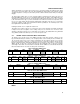
Table 45. Thermal Sensor SMBus Addressing
Address (Hex) Upper Address
1
Slot Select
8-bit Address Word on Serial Bus
SA1 SA2 b[7:0]
3Xh 0011 0 0 0011000Xb
0011 1 0 0011010Xb
5Xh 0101 0 Z
2
0101001Xb
0101 1 Z
2
0101011Xb
9Xh 1001 0 1 1001100Xb
1001 1 1 1001110Xb
NOTES:
1. Upper address bits are decoded in conjunction with the select pins.
2. A tri-state or “Z” state on this pin is achieved by leaving this pin unconnected.
Note that system management software must be aware of the slot number-dependent changes in the address
for the thermal sensor.
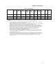
Table 46. Memory Device SMBus Addressing
Address
(Hex)
Upper
Address
1
Slot Select
Memory
Device
Select
R/W
Device Addressed
Bits 7-4
(SA1)
Bit 3
(SA0)
Bit 2
Bit 1
Bit 0
A0h/A1h 1010 0 0 0 X Scratch EEPROM 1
A2h/A3h 1010 0 0 1 X Processor Information ROM 1
A4h/A5h 1010 0 1 0 X Scratch EEPROM 2
A6h/A7h 1010 0 1 1 X Processor Information ROM 2
A8h/A9h 1010 1 0 0 X Scratch EEPROM 3
AAh/ABh 1010 1 0 1 X Processor Information ROM 3
ACh/ADh 1010 1 1 0 X Scratch EEPROM 4
AEh/AFh 1010 1 1 1 X Processor Information ROM 4
This addressing scheme is targeted for up to 4-way MP systems. More processors can be supported by using
a multiplexed (or separate) SMBus implementation.