
Datasheet

Pentium
®
III Xeon™ Processor at 500 and 550 MHz
28
Datasheet
NOTES:
1. Unless otherwise noted, these specifications are tested during manufacturing.
2. Not 100% tested. Specified by design characterization.
3. 1 ns can be added to the maximum TCK rise and fall times f or every 1MHz below 16.667MHz.
4. Referenced to TCK rising edge.
5. Referenced to TCK falling edge.
6. Valid delay timing for this signal is spec ified to 2.5V.
7. Non-Test Outputs and Inputs are the normal output or input signals (besides TCK, TRST#, TDI, TDO and
TMS). These timings correspond to the response of these signals due to TAP operations.
8. During Debug Port operation, use the normal specified timings rather than the TAP signal timings.
† Minimum time allowed between request cycles.
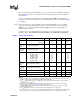
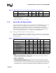
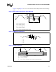
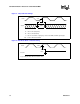
Table 16. System Bus AC Specifications (TAP Connection) at the Processor Core
1
T# Parameter Min Max Unit Figure Notes
T30: TCK Frequency 16.667 MHz
T31: TCK Period 60.0 ns 4
T32: TCK High Time 25.0 ns 4 @1.7 V
2
T33: TCK Low Time 25.0 ns 4 @0.7 V
2
T34: TCK Rise Time 3.0 5.0 ns 4 (0.7 V–1. 7V)
2, 3
T35: TCK Fall Time 3.0 5.0 ns 4 (1.7 V–0. 7V)
2, 3
T36: TRST# Pulse Width 40.0 ns 12 Asynchronous
2
T37: TDI, TMS Setup Time 5.0 ns 11 4
T38: TDI, TMS Hold Tim 14.0 ns 11 4
T39: TDO Valid Delay 1.0 10.0 ns 11 5, 6
T40: TDO Float Dela 25.0 ns 11 2, 5, 6
T41: All Non-Test Outputs Valid Delay 2.0 25.0 ns 11 5, 7, 8
T42: All Non-Test Inputs Setup Time 25.0 ns 11 2, 5, 7, 8
T43: All Non-Test Inputs Setup Time 5.0 ns 11 4, 7, 8
T44: All Non-Test Inputs Hold Time 13.0 ns 11 4, 7, 8
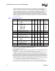
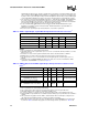
Table 17. SMBus Signal Group, AC Specifications at the Edge Fingers
T# Parameter Min Max Unit Figure Notes
T50: SMBCLK Frequency 100 KHz
T51: SMBCLK Period 10
µ
s5
T52: SMBCLK High Time 4.0
µ
s5
T53: SMBCLK Low Time 4.7
µ
s5
T54: SMBCLK Rise Time 1.0
µ
s5
T55: SMBCLK Fall Time 0.3
µ
s5
T56: SMBus Output Valid Delay 1.0
µ
s6
T57: SMBus Input Setup Time 250 ns 7
T58: SMBus Input Hold Time 0 ns 7
T59: Bus Free Time 4.7
µ
s†