
Datasheet

Pentium
®
III Xeon™ Processor at 500 and 550 MHz
26
Datasheet
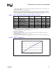
allowed between adjacent cycles. Positive or negative jitter of up to 250 ps is tolerated, but will result in up to
100 ps of AGTL+ I/O and CMOS timing degradation (i.e., timing parameters T7-9 and T11-13 will all increase
by 100 ps). Thus a system with jitter of 250 ps would need flight times that are 300 ps (100 ps additional jitter
+ 100 ps I/O timing degradation for both the source and receiver) better than a system with jitter of 150 ps.
7. The clock driver's closed loop jitter bandwidth should be less than 500 kHz (at -20dB). The bandwidth must
be set low to allow cascade connected PLL-based devices to track clock drivers with the specified jitter.
Therefore the bandwidth of the clock driver's output frequency-attenuation plot should be less than 500 kHz
measured at the -20 dB attenuation point. The test load should be 10 to 20 pF.
8. See the
100 MHz 2-Way SMP Pentium
®
III Xeon™ Processor/Intel
®
440GX AGPset AGTL+ Layout
Guidelines
or the
Pentium
®
III Xeon™ Processor/Intel
®
450NX PCIset AGTL+ Layout Guidelines
for
additional recommendations.
9. Not 100% tested. Specified by design characterization as a clock driver requirement.
NOTES:
1. These specifications are tested during manufacturing.
2. Valid delay timings for these signals at the processor core are correlated into 25 W ter mination to 1.5V and
with V
TT
set to 1 .5V.
3. A minimum of 3 clocks must be guaranteed between two active-to-inactive transitions of TRDY#.
4. RESET# can be asserted (active) asynchronously, but must be deasserted synchronously.
5. The signal at the processor core must transition monotonically through the overdrive region (2/3 V
TT
±
200mV).
6. After the bus ratio on A20M#, IGNNE# and LINT[1:0] are stable, V
CC
CORE
, V
CC
L2
and BCLK are within
specification, and PWRGOOD is asserted. See Figure 10.
NOTES:
1. These specifications are tested during manufacturing.
2. These signals may be driven asynchronously but must be driven synchronously in FRC mode
3. Valid delay timings for these signals are specified int o 100W to 2.5V.
4. To ensure recognition on a specific clock, the setup and hold times with respect to BCLK must be met.
5. INTR and NMI are only valid when the local APIC is disabled. LINT[1:0] are only valid when the local APIC is
enabled.
6. This specification only applies when the APIC is enabled and the LINT1 or LINT0 pin is configured as an
edge triggered interrupt with fixed delivery, otherwise specification T14 applies.
7. When driven inactive or after V
CC
CORE
, V
CC
L2
and BCLK become stable. PWRGOOD must remain below
V
IL_MAX
from Table 8 until all the voltage planes meet the voltage tolerance specifications i Table 5 and
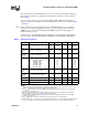
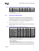
Table 12. AGTL+ Signal Groups, System Bus AC Specifications at the Processor Core
1
R
L
= 25
Ω
Terminated to 1.5 V
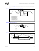
T# Parameter Min Max Unit Figure Notes
T7: AGTL+ Output Valid Delay -0.07 2.7 ns 6 2
T8: AGTL+ Input Setup Time 1.75 ns 7 3, 4, 5
T9: AGTL+ Input Hold Time 0.62 ns 7 5
T10: RESET# Pulse Width 1.00 ms 10 6
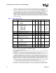
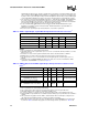
Table 13. CMOS, TAP, Clock and APIC Signal Groups, AC Specifications at the Processor
Core
1, 2
T# Parameter Min Max Unit Figure Notes
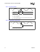
T11: CMOS Output Valid Delay 1 8 ns 6 3
T12: CMOS Input Setup Time 4 ns 7 4, 5
T13: CMOS Input Hold Tim 1 ns 7 4
T14: CMOS Input Pulse Width, except
PWRGOOD and LINT[1:0]
2 BCLKs 6 Active and Inactive states
T14B: LINT[1:0] Input Pulse Width 6 BCLKs 5 6
T15: PWRGOOD Inactive Pulse Width 10 BCLKs
6
11
7, 8