
Datasheet


Pentium
®
III Xeon™ Processor at 500 and 550 MHz
Datasheet
19
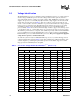
NOTES
1. The BR0# pin is the only BREQ# signal that is bi-directional. The internal BREQ# signals are mapped onto
BR# pins based on a processor’s agent ID. See Section 9.0 for more information.
2. For information on these signals, see Section 9.0.
3. These signals are specified fo r 2.5V operation.
4. V
CC
CORE
is the power supply for the Pentium
®
III Xeon™ processor core.
V
CC
L2
is the power supply for the L2 cache memory.
VID_CORE[4:0], and VID_L2[4:0] pins are described in Table 2.
V
TT
is used for the AGTL+ termination.
V
SS
is system ground.
V
CC
TA P
is the TAP supply.
V
CC
SMB
US
is the SM bus supply.
Reserved pins must be left unconnected. Do not connect to each other.
Test Pins are described in Section 2.6.
Other signals are described in Section 9.0.
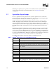
2.7.1 Asynchronous vs. Synchronous for System Bus Signals
All AGTL+ signals are synchronous to BCLK. All of the CMOS, Clock, APIC, and TAP signals
can be applied asynchronously to BCLK, except when running two processors as an FRC pair.
Synchronization logic is required on signals going to both processors in order to run in FRC mode.
The TAP logic can not be used while a processor is running in an FRC pair, and the TAP signals
should therefore be at the appropriate inactive levels for FRC operation.
Also note the timing requirements for FRC mode operation. With FRC enabled, PICCLK must be
1/4 the frequency of BCLK, synchronized with respect to BCLK, and must always lag BCLK as
specified in Table 15 and Figure 8.
All APIC signals are synchronous to PICCLK. All TAP signals are synchronous to TCK. All
SMBus signals are synchronous to SMBCLK. TCK and SMBCLK may always be asynchronous to
all other clocks.
2.8 Test Access Port (TAP) Connection
Depending on the voltage levels supported by other components in the Test Access Port (TAP)
logic, it is recommended that the Pentium
III
Xeon processors be first in the TAP chain and
followed by any other components within the system. A voltage translation buffer should be used to
drive the next device in the chain unless a 3 .3V o r 5V component is used that is capable of
accepting a 2.5V input. Similar considerations must be made for TCK, TMS, and TRST#.
Multiple copies of each TAP signal may be required if multiple voltage levels are needed within a
system.
Note:
TDI is pulled up to V
CC
TAP
with ~150
Ω
on the Pentium
III
Xeon processor cartridge. An open
drain signal driving this pin must be able to deliver sufficient current to drive the signal low. Also,
no resistor should exist in the system design on this pin as it would be in parallel with this resistor
A Debug Port is described in Section 8.0. The Debug Port must be placed at the start and end of the
TAP chain with TDI to the first component coming from the Debug Port and TDO from the last
component going to the Debug Port. In an MP system, be cautious when including an empty
SC330 connector in the scan chain. All connectors in the scan chain must have a processor or
termination card installed to complete the chain between TDI and TDO or the system must support
a method to bypass the empty connectors; SC330 terminator substrates should tie TDI directly to
TDO. (See Section 8.0 for more details.)