
Datasheet


Pentium
®
III Xeon™ Processor at 500 and 550 MHz
18
Datasheet
When tying
any
signal to power or ground, a resistor will also allow for system testability. For
correct operation when using a logic analyzer interface, refer to Section 8.0 for design
considerations.
2.7 System Bus Signal Groups
In order to simplify the following discussion, the system bus signals have been combined into
groups by buffer type.
All system bus outputs should be treated as open drain
and require a high
level source provided externally by the termination or pull-up resistor.
AGTL+ input signals have differential input buffers, which use 2/3 V
TT
as a reference level.
AGTL+ output signals require termination to 1.5V. I n this document, the term “AGTL+ Input”
refers to the AGTL+ input group as well as the AGTL+ I/O group when receiving. Similarly,
“AGTL+ Output” refers to the AGTL+ output group as well as the AGTL+ I/O group when driving.
The AGTL+ buffers employ active negation for one clock cycle after assertion to improve rise
times.
The CMOS, Clock, APIC, and TAP inputs can each be driven from ground to 2.5V. The CMOS,
A PIC, and T A P o u t p u ts ar e op e n drain and should be p u lled high t o 2.5V. This e n sures no t o n l y
correct operation for current Pentium
III
Xeon processors, but compatibility for future Pentium
III
Xeon processor products as well. There is no active negation on CMOS outputs. ~150
Ω
resistors
are expected on the PICD[1:0] lines. Timings are specified into the load resistance as defined in the
AC timing tables. See Section 8.0 for design considerations for debug equipment.
The SMBus signals should be driven using standard 3.3 V CMOS logic levels.
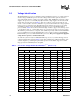
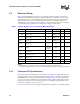
Table 3. Pentium
®
III Xeon™ Processor System Bus Pin Groups
Group Name Signals
AGTL+ Input BPRI#, BR[3:1]#
1
, DEFER#, RESET#, RS[2:0]#, RSP#, TRDY#
AGTL+ Output PRDY#
AGTL+ I/O
A[35:03]#, ADS#, AERR#, AP[1:0]#, BERR#, BINIT#, BNR#, BP[3:2]#, BPM[1:0]#, BR0#
1
,
D[63:00]#, DBSY#, DEP[7:0]#, DRDY#, FRCERR, HIT#, HITM#, LOCK#, REQ[4:0]#, RP#
CMOS Input
A20M#, FLUSH#, IGNNE#, INIT#, LINT0/INTR, LINT1/NMI, PREQ#, PWRGOOD
2
, SMI#,
SLP#
2
, STPCLK#
CMOS Output FERR#, IERR#, THERMTRIP#
2
System Bus
Clock
bclk
APIC Clock picclk
APIC I/O
3
picd[1:0]
TAP Input tck, tdi, tms, trst#
TA P Out pu t
3
TDO
SMBus Interface SMBDAT, SMBCLK, SMBALERT#, WP
Power/Other
4
V
CC
CORE
, V
CC
L2
, V
CC
TA P
, V
CC
SMB
US
,
VID_L2[4:0], VID_CORE[4:0], V
TT
, V
SS
,
TEST_25_A62, TEST_VCC_CORE, TEST_VSS, PWR_EN[1:0]
2
, RESERVED_XXX,
SA[2:0], SELFSB[1:0]