
Datasheet


Pentium
®
III Xeon™ Processor at 500 and 550 MHz
Datasheet
13
when the part is powering on, or entering/exiting low power states, is provided on the voltage
regulation module (VRM) defined in the
VRM 8.2 DC–DC Converter Design Guidelines
and the
VRM 8.3 DC–DC Converter Design Guidelines
. The input to V
CC
CORE
should be capable of
delivering a recommended minimum d
ICC
CORE
/dt defined in Table 6 while maintaining the
required tolerances defined in Table 5. See the
Pentium
®
III
Xeon™ Processor Power Distribution
Guidelines
.
2.3.2 Level 2 Cache Decoupling
Regulator solutions need to provide bulk capacitance with a low Effective Series Resistance (ESR)
in order to meet the tolerance requirements for V
CC
L2
. Use similar design practices as those
recommended for V
CC
CORE
. See the
Pentium
®
III
Xeon™ Processor Power Distribution
Guidelines
.
2.3.3 System Bus AGTL+ Decoupling
The Pentium
III
Xeon processor contains high frequency decoupling capacitance on the processor
substrate; bulk decoupling must be provided for by the system baseboard for proper AGTL+ bus
operation. High frequency decoupling may be necessary at the SC330 connector to further improve
signal integrity if noise is picked up at the connector interface. See the
Pentium
®
III
Xeon™
Processor Power Distribution Guidelines
.
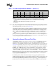
2.4 System Bus Clock and Processor Clocking
The BCLK input directly controls the operating speed of the system bus interface. All system bus
timing parameters are specified with respect to the rising edge of the BCLK input, measured at the
processor core. The Pentium
III
Xeon processor core frequency must be configured during Reset by
using the A20M#, IGNNE#, LINT[1]/NMI, and LINT[0]/INTR pins (see Table 1). The value on
these pins during Reset determines the multiplier that the Phase Lock Loop (PLL) will use for the
internal core clock. See the
P6 Family of Processors Hardware Developer's Manual
for the
definition of these pins during reset and the operation of the pins after reset.
Note:
The frequency multipliers supported are shown in Table 1; other combinations will not be validated
nor supported by Intel. Also, each multiplier is only valid for use on the product of the frequency
indicated in Table 1.
Clock multiplying within the processor is provided by the internal PLL, requiring a constant
frequency BCLK input. The BCLK frequency ratio cannot be changed dynamically during normal
operation or any low power modes. The BCLK frequency ratio can be changed when RESET# is
active, assuming that all Reset specifications are met.
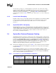
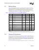
Table 1. Core Frequency to System Bus Multiplier Configuration
Multiplication of Processor
Core Frequency to System
Bus Frequency
Product Supported
on
LINT[1] LINT[0] A20M# IGNNE#
1/2 Reset only L L L L
1/3 Not Supported L L L H
1/4 Not Supported L L H L
1/5 500, 550 MHz L L H H