
Intel Pentium M Processor Datasheet


Package Mechanical Specifications and Pin Information
60 Intel
®
Pentium
®
M Processor Datasheet
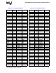
M2 DBSY# Common Clock Input/Output
M3 TRDY# Common Clock Input
M4 VSS Power/Other
M5 VSS Power/Other
M6 VCCP Power/Other
M21 VSS Power/Other
M22 VCCP Power/Other
M23 D[24]# Source Synch Input/Output
M24 VSS Power/Other
M25 D[28]# Source Synch Input/Output
M26 D[19]# Source Synch Input/Output
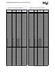
N1 VCCA[2] Power/Other
N2 ADS# Common Clock Input/Output
N3 VSS Power/Other
N4 BR0# Common Clock Input/Output
N5 VCCP Power/Other
N6 VSS Power/Other
N21 VCCP Power/Other
N22 VSS Power/Other
N23 VSS Power/Other
N24 D[27]# Source Synch Input/Output
N25 D[30]# Source Synch Input/Output
N26 VSS Power/Other
P1 REQ[3]# Source Synch Input/Output
P2 VSS Power/Other
P3 REQ[1]# Source Synch Input/Output
P4 A[3]# Source Synch Input/Output
P5 VSS Power/Other
P6 VCCP Power/Other
P21 VSS Power/Other
P22 VCCP Power/Other
P23 VCCQ[0] Power/Other
P24 VSS Power/Other
P25 COMP[0] Power/Other Input/Output
P26 COMP[1] Power/Other Input/Output
R1 VSS Power/Other
R2 REQ[0]# Source Synch Input/Output
R3 A[6]# Source Synch Input/Output
R4 VSS Power/Other
Table 21. Pin Listing by Pin Number
Pin
Number
Pin Name
Signal Buffer
Type
Direction
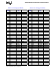
R5 VCCP Power/Other
R6 VSS Power/Other
R21 VCCP Power/Other
R22 VSS Power/Other
R23 D[39]# Source Synch Input/Output
R24 D[37]# Source Synch Input/Output
R25 VSS Power/Other
R26 D[38]# Source Synch Input/Output
T1 REQ[4]# Source Synch Input/Output
T2 REQ[2]# Source Synch Input/Output
T3 VSS Power/Other
T4 A[9]# Source Synch Input/Output
T5 VSS Power/Other
T6 VCCP Power/Other
T21 VSS Power/Other
T22 VCCP Power/Other
T23 VSS Power/Other
T24 DINV[2]# CMOS Input/Output
T25 D[34]# Source Synch Input/Output
T26 VSS Power/Other
U1 A[13]# Source Synch Input/Output
U2 VSS Power/Other
U3 ADSTB[0]# Source Synch Input/Output
U4 A[4]# Source Synch Input/Output
U5 VCC Power/Other
U6 VSS Power/Other
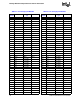
U21 VCCP Power/Other
U22 VSS Power/Other
U23 D[35]# Source Synch Input/Output
U24 VSS Power/Other
U25 D[43]# Source Synch Input/Output
U26 D[41]# Source Synch Input/Output
V1 VSS Power/Other
V2 A[7]# Source Synch Input/Output
V3 A[5]# Source Synch Input/Output
V4 VSS Power/Other
V5 VSS Power/Other
V6 VCC Power/Other
V21 VSS Power/Other
Table 21. Pin Listing by Pin Number
Pin
Number
Pin Name
Signal Buffer
Type
Direction