
Intel Pentium M Processor with 2-MB L2 Cache and 533-MHz Front Side Bus Datasheet

24 Datasheet
Electrical Specifications
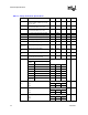
NOTES:
1. Unless otherwise noted, all specifications in this table apply to all processor frequencies.
2. Crossing Voltage is defined as absolute voltage where rising edge of BCLK0 is equal to the falling edge of
BCLK1.
3. Threshold Region is defined as a region entered about the crossing voltage in which the differential receiver
switches. It includes input threshold hysteresis.
4. For Vin between 0 V and V
H
.
5. Cpad includes die capacitance only. No package parasitics are included.
6. V
CROSS
is defined as the total variation of all crossing voltages as defined in note 2.
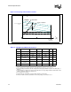
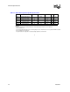
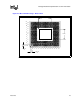
Figure 3-2. Deep Sleep VCC and ICC Load Line
I
CC
max
{HFM|LFM}
V
CC
[V]
Slope= -3.0 mV/A
Vcc
nom {HFM|LFM}
- 1.2%
+/-1.5% from Nominal =VR Error
10mV= RIPPLE
I
CC
[A]
0
Deep Sleep
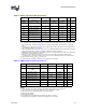
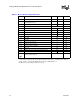
Table 3-6. FSB Differential BCLK Specifications
Symbol Parameter Min Typ Max Unit Notes
1
V
L
Input Low Voltage 0 V
V
H
Input High Voltage 0.660 0.710 0.85 V
V
CROSS
Crossing Voltage 0.25 0.35 0.55 V 2
V
CROSS
Range of Crossing
Points
N/A N/A 0.140 V 6
V
TH
Threshold Region V
CROSS
-0.100 V
CROSS
+0.100 V 3
ILI Input Leakage
Current
± 100 µA 4
Cpad Pad Capacitance 1.8 2.3 2.75 pF 5