
Intel Pentium M Processor Datasheet


Intel
®
Pentium
®
M Processor Datasheet 37
Electrical Specifications
NOTES:
1. Unless otherwise noted, all specifications in this table apply to all processor frequencies.
2. Crossing Voltage is defined as absolute voltage where rising edge of BCLK0 is equal to the falling edge of
BCLK1.
3. Threshold Region is defined as a region entered about the crossing voltage in which the differential receiver
switches. It includes input threshold hysteresis.
4. For Vin between 0 V and V
H
.
5. Cpad includes die capacitance only. No package parasitics are included.
6.
∆V
CROSS
is defined as the total variation of all crossing voltages as defined in note 2.
NOTES:
1. Unless otherwise noted, all specifications in this table apply to all processor frequencies.
2. V
IL is defined as the maximum voltage level at a receiving agent that will be interpreted as a logical low value.
3. V
IH is defined as the minimum voltage level at a receiving agent that will be interpreted as a logical high
value.
4. This is the pull down driver resistance. Measured at 0.31*VCCP. R
ON
(min) = 0.38*R
TT,
R
ON
(typ) = 0.45*R
TT,
R
ON
(max) = 0.52*R
TT.
5. GTLREF should be generated from VCCP with a 1% tolerance resistor divider. The VCCP referred to in these
specifications is the instantaneous VCCP.
6. R
TT
is the on-die termination resistance measured at V
OL
of the AGTL+ output driver. Measured at
0.31*VCCP. R
TT
is connected to VCCP on die.
7. Specified with on die R
TT
and R
ON
are turned off.
8. Cpad includes die capacitance only. No package parasitics are included.
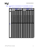
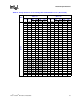
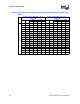
Table 14. System Bus Differential BCLK Specifications
Symbol Parameter Min Typ Max Unit Notes
1
V
L
Input Low Voltage 0 V
V
H
Input High Voltage 0.660 0.710 0.850 V
V
CROSS
Crossing Voltage 0.25 0.35 0.55 V 2
∆V
CROSS
Range of Crossing Points N/A N/A 0.140 V 6
V
TH
Threshold Region V
CROSS
-0.100 V
CROSS
+0.100 V 3
I
LI Input Leakage Current ± 100 µA 4
Cpad Pad Capacitance 1.8 2.3 2.75 pF 5
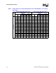
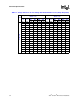
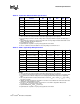
Table 15. AGTL+ Signal Group DC Specifications
Symbol Parameter Min Typ Max Unit Notes
1
VCCP I/O Voltage 0.997 1.05 1.102 V
GTLREF Reference Voltage
2/3 VCCP -
2%
2/3 VCCP
2/3 VCCP +
2%
V5
V
IH Input High Voltage GTLREF+0.1 VCCP+0.1 V 3,5
V
IL Input Low Voltage -0.1 GTLREF-0.1 V 2
V
OH Output High Voltage VCCP 5
R
TT
Termination Resistance 47 55 63 Ω 6
R
ON Buffer On Resistance 17.7 24.7 32.9 W 4
I
LI Input Leakage Current ± 100 µA 7
Cpad Pad Capacitance 1.8 2.3 2.75 pF 8