
Guide


Thermal and Mechanical Design
58 Intel® Xeon® Processor E7 2800/4800/8800 v2 Product Family
Thermal/ Mechanical Specifications and Design Guide
2.4.5.7 Strain Guidance
Intel provides manufacturing strain guidance commonly referred to as Board Flexure
Initiative or BFI Strain Guidance. The BFI strain guidance apply only to transient bend
conditions seen in board manufacturing assembly environment with no ILM, for
example during In Circuit Test. BFI strain guidance limits do not apply once ILM is
installed. It should be noted that any strain metrology is sensitive to boundary
conditions.
Intel recommends the use of BFI to prevent solder joint defects from occurring in the
test process. For additional guidance on BFI, see Manufacturing With Intel®
Components - Strain Measurement for Circuit Board Assembly, also referred as BFI
MAS (Manufacturing Advantage Services) and BFI STRAIN GUIDANCE SHEET
(LGA2011-1 socket). Consult your Intel Customer Quality Engineer for additional
guidance in setting up a BFI program in your factory.
When the ILM is attached to the board, the boundary conditions change and the BFI
strain limits are not applicable. The ILM, by design, increases stiffness in and around
the socket and places the solder joints in compression. Intel does not support strain
metrology with the ILM assembled
2.4.5.8 Board Deflection
Exceeding the maximum Board Deflection called out in Table 2-5, “Socket Loading and
Deflection Specifications”, may result in socket solder joint failure. Board deflection
under the LGA2011-1 socket will be kept to an acceptable level by adhering to the
following conditions:
1. Using the Intel reference ILM and back plate
2. Maintaining compliance to maximum load values
Placement of board-to-chassis mounting holes also impacts board deflection and
resultant socket solder ball stress. Customers need to assess shock for their designs as
their heatsink retention, heatsink mass and chassis mounting holes may vary.
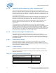
Table 2-18. Recommended Land Pattern for LGA2011-1 Socket
Pad Description Recommendation Details
NCTF Pads - 43 pads in
the four corners
• Oblong partially SMD Pad (20 x 17 mil) oriented at 45° to the socket edge.
• The pad end closest to the center of the socket should have the Solder Resist
Opening (SRO) of 17 ±1 mil. This is a critical to function dimension.
• A thick trace ideally oriented at 45° toward the package corner and parallel to
the long axis of the pad is required for optimal solder joint reliability (SJR)
protection.
• Pads affected:
(SE) A53, B54, C55, D56, E57, F58, A51, B52, C53, G57, H58
(NE) CU1, CW1, CY2, DA3, DB4, DC5, DD6, DE7, DF8, DB2, DC3
(NW) E1, D2, C3, A5, G1, F2, E3, D4, C5, B6, A7
(SW) DF52, DE53, DD54, DC55, DB56, DA57, CY58, CV58, DE55, DB58
Critical to Function Pads
along the socket sides.
• Oblong partially SMD Pad (20 x 17mil) oriented perpendicular to the socket
edge.
• The pad end closest to the center of the socket should have the SRO of
17±1 mil. This is a critical to function dimension.
• A thick trace oriented parallel to the long axis of the pad is required for
optimal SJR protection.
All other Critical to
function pads.
• Circular MD
• 17 ±1 mil Solder Resist Opening (SRO). This is a critical to function dimension