
ITP700 Debug Port Design Guide


R
ITP700 Debug Port Design Guide 61
pairs from the system clock source. One pair is for the motherboard debug port, and the other
is for the ITP_BCLK(p/n) pins on the processor socket. The routing guidelines for the
motherboard based debug port are defined in Chapter 1. The processor socket
ITP_BCLK(p/n) pins have the same routing and termination requirements as a processor
clock pair. If an ITP clock pair is to be used for more than one load, all routing requirements
for both loads must be met, and simulations must be conducted to ensure that a quality clock
is provided at both loads.
Clarification 1. The BPM[5:0]# and RESET# traces should be terminated to the processor VCC
voltage on both ends of the transmission line similar to the system bus. For systems that enable on-
die termination of the system bus, understand that the Pentium
4 processor does not provide on-die
termination of the BPM[5:0]# and RESET# signals. Consult individual chipset documentation to
assess if a chipset component should be connected to the BPM[5:0]# , RESET#, or JTAG signals.
Clarification 2. The system clock of the Intel
Xeon Processor with 512-KB L2 cache at 2.20, 2.0,
and 1.80 GHz DP and Intel Xeon processor MP servers reference BCLK[1:0] where BCLK0 is the
rising edge for the beginning any transaction and BCLK1 is the falling edge. The ITP uses
BCLK[p/n] where BCLKp is the rising edge and BCLKn is the falling edge for the beginning of
any transaction. All routing Rules for the BCLK signals do not change.
Note: The BPM[5:0]# routing has changed. For previous processors, it was recommended to have
BPM0# and BPM2# tied as well as BPM1# and BPM3# tied together. This is no longer the case.
It is now recommended that each BPM[5:0]# line be routed directly from the processor to the
debug port.
7.1.1 ITP Clock Routing for Intel
®
Pentium
®
4 Processor
These specifications pertain to the ITP clock routing for the Pentium 4 processor with 512-KB L2
cache on 0.13 micron process. There are essentially two options for providing a clock to the ITP.
Option A uses the CK408 clock generator, a choice used in many designs. Option B is only
available for B0 silicon or greater, with the new ITPCLKOUT[1:0] pins implemented on the
processor. The ITPCLKOUT[1:0] provides a buffered version of BCLK to the ITP. Both routing
options as described below will allow for the use of an ITP interposer. ITP interposers are often
used in manufacturing test or in place of an on-board ITP.
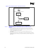
7.1.1.1 Option A) Using the CK408 Clock Generator
1. Route the BCLK pair from the CK408 to both the ITPCLK[1:0] on the processor and the
BCLK[n:p] on the ITP debug port. See Figure below.
2. Terminate ITPCLKOUT[1:0] on the processor (if applicable) with separate1 kΩ pull-up
resistors to VCC_CORE.
1