
603 Pin Socket Design Guidelines

603 Pin Socket Design Guidelines
R
12
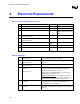
3.3.4.3. Contact Area Plating:
76.2µmm (min) gold plating over 127µmm (min) nickel underplate in critical contact areas (area on
socket contacts where processor pins will mate). No contamination by solder in the contact area is
allowed during solder reflow.
3.3.4.4. Solder Ball/Surface Mount Feature Attachment Area Plating:
381µmm (min) Tin/Lead (typically 85±5Sn/15Pb).
3.3.4.5. Solder Ball/Surface Mount Feature Characteristics:
Tin/Lead (63/37 ± 0.5% Sn),.
3.3.4.6. Lubricants:
Final assembly shall not have any lubricants on the socket contacts.
3.3.5. Environmental Concerns Requirements:
Cadmium shall not be used in the painting or plating of the socket.
CFCs and HFCs shall not be used in manufacturing the socket.
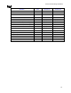
3.4. Visual Inspection:
The visual inspection criteria will be OEM specific.
3.5. Socket Manufacturability Requirements:
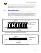
3.5.1. Lever Design Requirements
• Lever closed direction – right
• Actuation direction called out in Figure 9-5 (Appendix A.5)
• 135° lever travel max
• Pivot point in the center of the actuation area on the top of the socket (see Figure 9-6 -
Appendix A.6)
• Keep in drawing Figure 9-6 - Appendix A.6
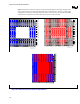
3.5.2. Socket Engagement/Disengagement Force:
Less than a force of 4.5Kg or a torque of 112mm-Kg(e.g. using a 25.4mm diameter screwdriver palming
the screwdriver "Power Grip" not finger tips) to engage/disengage using the actuation tool, movement of
the cover limited to the plane parallel to the motherboard. The processor package must not be utilized
in the actuation of the socket. The actuation tool must be readily available on the open market. Any