
Voltage Regulator Module (VRM) and Enterprise Voltage Regulator-Down (EVRD) 10.2 Design Guidelines

Voltage Regulator Module (VRM) and Enterprise Voltage 9
Regulator-Down (EVRD) 10.2 Design Guidelines
2 Output Voltage Requirements
2.1 Voltage and Current - REQUIRED
There will be independent selectable voltage identification (VID) codes for the core voltage
regulator. The regulator’s 6-bit code (VID) will be provided by the processor to the VRM/EVRDs,
which will determine a reference output voltage, as described in Section 3.2. Section 2.2 and
Section 2.3 specify deviations from the VID reference voltage.
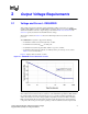
The load line tolerance in Section 2.2 shows the relationship between Vcc and Icc for the
processor.
The VRM/EVRD is required to support the following:
• A maximum continuous load current (Icc
TDC
) of 130A.
• A maximum load current (Icc
MAX
) of 150A peak.
• A maximum load current step (Icc
STEP
), within a 1 µs period, of 100A.
• A maximum current slew rate (dIcc/dt) of 1200 A/µs at the pins of the processor (refer to
Table 2-2 for more information).
Figure 2-1displays the load current over time.
NOTE: Voltage regulator thermal protection circuitry should not trip for load currents greater than Icc
TDC
The continuous load current can also be referred to as the Thermal Design Current (TDC). TDC is
the sustained (DC equivalent) current that the processor is capable of drawing indefinitely and
defines the current to use for the voltage regulator temperature assessment. At TDC, switching
FETs reach maximum allowed temperature and may heat the baseboard layers and neighboring
components. The envelope of the system operating conditions establishes actual component and
Figure 2-1. VRM/EVRD 10.2 Load Current vs. Time