
Voltage Regulator Module (VRM) and Enterprise Voltage Regulator-Down (EVRD) 10.2 Design Guidelines


4 Voltage Regulator Module (VRM) and Enterprise Voltage
Regulator-Down (EVRD) 10.2 Design Guidelines
8.6 Shock and Vibration - PROPOSED .................................................................................. 34
8.7 Electromagnetic Compatibility - PROPOSED ................................................................... 34
8.8 Reliability - PROPOSED ................................................................................................... 34
8.9 Safety - PROPOSED ........................................................................................................ 34
9 Lead Free (Pb Free).........................................................................................................35
Figures
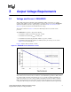
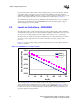
2-1 VRM/EVRD 10.2 Load Current vs. Time............................................................................. 9
2-2 VRM/EVRD 10.2 Socket Load Line .................................................................................. 10
2-3 Power-On Sequence Block Diagram ................................................................................ 12
2-4 Power-On Sequence Timing Diagram .............................................................................. 13
2-5 Processor Transition States.............................................................................................. 14
2-6 Dynamic VID Transition States Illustration........................................................................ 14
2-7 64-bit Intel
®
Xeon™ Processor MP with up to 8MB L3 Cache Load Model...................... 16
2-8 64-bit Intel® Xeon™ Processor MP with up to 1MB L2 Cache Load Model ..................... 16
7-1 VRM 10.2 Module and Connector..................................................................................... 32
Tables
2-1 LL0, LL1 Codes................................................................................................................. 11
2-2 Recommended Decoupling and Other Specifications for Supported Processors............. 15
2-3 VRM 10.2 Decoupling Capacitor Recommendations........................................................ 16
3-1 OUTEN Specifications ...................................................................................................... 19
3-2 VID [5:0] Specifications....................................................................................................19
3-3 Voltage Identification (VID) ............................................................................................... 20
3-4 LL0, LL1 Specifications..................................................................................................... 21
6-1 Vcc_PWRGD Specifications ............................................................................................. 27
6-2 VR_hot# Specifications..................................................................................................... 27
6-3 VRM_pres Specifications.................................................................................................. 28
7-1 VRM 10.2 Connector Part Number and Vendor Name ..................................................... 29
7-2 VRM 10.2 Connector Pin Descriptions.............................................................................. 30
7-3 VRM 10.2 Pin Assignments .............................................................................................. 31