
Voltage Regulator Module (VRM) and Enterprise Voltage Regulator-Down (EVRD) 10.2 Design Guidelines

Voltage Regulator Module (VRM) and Enterprise Voltage 11
Regulator-Down (EVRD) 10.2 Design Guidelines
Output Voltage Requirements
2.3 Voltage Tolerance - REQUIRED
The voltage ranges shown in Section 2.2 include the following tolerances:
• Initial DC output voltage set-point error.
• Output ripple and noise.
• No-load offset centering error.
• Current sensing and droop errors.
• Component aging effects.
• Full ambient temperature range and warm up.
• Dynamic output changes from minimum-to-maximum and maximum-to-minimum load
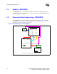
should be measured at the point of regulation (recommended to be at the center of the
processor socket) using an oscilloscope set to a 20-MHz bandwidth. When measuring the
response of the die voltage to dynamic loads, use the VCCSENSE and VSSSENSE pins on the
processor socket with an oscilloscope set to 100 MHz bandwidth and with probes that are
1.5 pF maximum and 1M Ω minimum impedance.
• Variations of the input voltage.
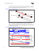
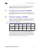
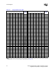
Table 2-1. LL0, LL1 Codes
LL0 LL1 Processor
00Reserved
0 1 64-bit Intel
®
Xeon™ processor MP with up to 8MB L3 cache, 64-bit Intel
®
Xeon™ processor
MP with 1MB L2 cache and mPGA604 Die Load Line
10Reserved
11Reserved
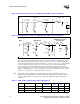
LL0 LL1 Vcc Tolerance / Load Line Units Notes
00Vcc
MAX
= Reserved V
Vcc
MIN
= Reserved
01Vcc
MAX
= VID (V) – 1.25 m • Icc (A) V 64-bit Intel® Xeon™
processor MP with up to
8MB L3 cache and 64-bit
Intel® Xeon™ processor
MP with 1MB L2 cache
Vcc
MIN
= VID (V) – 1.25 m • Icc (A) – 40 mV
10Vcc
MAX
= Reserved V
Vcc
MIN
= Reserved
11Vcc
MAX
= Reserved V
Vcc
MIN
= Reserved