
ITP700 Debug Port Design Guide


R
88 ITP700 Debug Port Design Guide
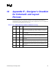
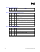
Table 42. Part 2: TDI/TDO Connectivity
PASS FAIL Don’t
Care
ISSUE
Is the connectivity of TDI/TDO around the scan chain correct?
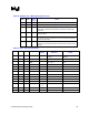
Table 43. TDI/TDO Connectivity Through Bypass Circuitry
PASS FAIL Don’t
Care
ISSUE
If FETs are used for bypass, is there a risk of capacitive effects on timing
budgets?
If FETs are used for bypass, is there a risk of signal leakage through the
body diode of the FET?
If QuickSwitches are used for bypass, is there any risk of signal corruption
near the VCC and GND rails of the QuickSwitch that might affect noise
margins?
Will the Bypass Method completely remove a scan agent from the scan
chain? (Please note that this may not be a requirement for all systems.
Is there any chance of dual pull-ups on a TDI/TDO path due to bypass
logic?
Is there any chance of NO pull-ups on a TDI/TDO path due to bypass
logic?
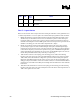
Table 44. Part 3: TCK / TMS Implementation
PASS FAIL Don’t’
Care
ISSUE
Is there a single pull-down on TCK?
Is there a single pull-up on TMS?
If any extra locations for on-board filtering of TCK or TMS are in the
schematic, they must listed as Do Not Stuff.
Hysterisis should be implemented for all receivers of TCK
TCK should be routed to FBO for un-buffered implementations.