
Intel Xeon Processor and Intel E7500/E7501Chipset Compatible Platform Design Guide

Intel
®
Xeon™ Processor and Intel
®
E7500/E7501 Chipset Compatible Platform Design Guide 93
Memory Interface Routing Guidelines
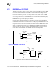
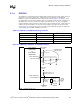
6.6 Clock Enable Routing
The MCH provides a single clock enable (CKE) signal. This signal is used during initialization to
indicate that valid power and clocks are being applied to the DIMMs. Because the CKE signal has
higher loading, it requires a lower impedance. The recommended impedance for the CKE signal is
40 Ω. This can be achieved using a 7.5-mil wide trace on the recommended stack-up
(refer to Figure 6-5). It is acceptable to route the CKE signal 5-mils wide and 5-mils spacing when
breaking out of the MCH. However, the trace must be widened to 7.5 mils before widening the
spacing to 15 mil. The CKE signal requires a parallel termination resistor (Rtt) to DDR VTERM
placed as close to the last DIMM connector as possible.
NOTES:
1. On a compatible motherboard, use a 33.2 Ω for an E7500 chipset MCH and a 39.2 Ω for an E7501 chipset
MCH.
NOTE: Indicated lengths measure from the MCH component pin to the DIMM connector pin.
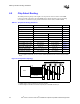
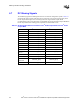
Table 6-8. Clock Enable Routing Guidelines
Parameter 3-DIMM Solution 4-DIMM Solution Reference
Signal Group CKE
Topology Daisy Chain with Stubs Figure 6-11
Reference Plane Ground Figure 6-5
Trace Impedance (Z
0
) 40 Ω ± 10% 40 Ω ± 10% Table 6-2
Nominal Trace Width 7.5 mil 7.5 mil Figure 6-5
Nominal Trace Spacing 15 mil 15 mil Figure 6-5
MCH to DIMM1 Trace Length 1.8” to 6.0” 1.8” to 6.0” Figure 6-11
DIMM to DIMM Trace Length 0.8” to 1.2” 0.8” to 1.2” Figure 6-11
CKE_x Stub Trace Length < 300 mil < 300 mil Figure 6-11
DIMM to Rtt Trace Length < 0.8” < 0.8” Figure 6-11
Termination Resistor (Rtt) 39.2
Ω ± 1% / 33.2 Ω ± 1%
1
34.8 Ω ± 1% Figure 6-11
MCH Breakout Guidelines 5/5, < 500 mil 5/5, < 500 mil
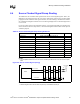
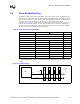
Figure 6-11. CKE Topology
CKE_x
MCH
DDR VTERM
(1.25 V)
DIMMs
DIMM to
DIMM
Rtt
DIMM to
DIMM
DIMM to
DIMM
MCH to DIMM1
DIMM
to Rtt
CKE_x Stub