
Intel Xeon Processor and Intel E7500/E7501Chipset Compatible Platform Design Guide

Intel
®
Xeon™ Processor and Intel
®
E7500/E7501 Chipset Compatible Platform Design Guide 63
System Bus Routing Guidelines
System Bus Routing Guidelines 5
This chapter covers the system bus source synchronous (data, address, and associated strobes) and
common clock signal routing. Table 5-1 lists the signals and their corresponding signal types.
NOTES:
1. These signals do not have on-die termination on the processor. They must be terminated properly on the
motherboard. If the signal is not connected, it must be pulled to the appropriate voltage level through a
1 k
Ω ± 5% resistor.
2. Intel Xeon processors use only BR0# and BR1#.
3. The processor uses these signals as ‘wired-OR’. They may be driven simultaneously by multiple agents.
4. The value of these pins during the active edge of RESET# determine processor configuration options.
5. SM_VCC/VID_VCC has critical power sequencing requirements documented in Section 11.2.6.
6. Critical terminations and routing for RESET#, BPM[5:0]#, TAP signals and all debug port signals are found in
the
ITP700 Debug Port Design Guide.
7. These signals are only defined and driven by the Intel Xeon processor with 533 MHz system bus.
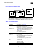
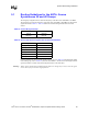
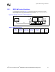
The dual-processor topology requires that the MCH be at one end of the bus, Processor 0 be at the
other end of the bus, and Processor 1 be in the middle of the bus (Figure 5-1). The motherboard
routing to Processor 1 must not create a stub on the system bus signals at the socket. This requires
routing into the socket and back out of the socket. For Uni-Processor (UP) operation, the single
processor must be installed in the Processor 0 socket, at the end of the bus. Figure 5-1 shows the
recommended dual processor topology used for system bus routing.
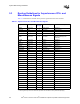
Table 5-1. System Bus Signal Groups
Signal Group Type Signals
AGTL+ Common Clock Input Synchronous to BCLK
BPRI#, BR[3:1]#
1,2
, DEFER#, RESET#
1,6
,
RS[2:0]#, RSP#, TRDY#
AGTL+ Common Clock I/O Synchronous to BCLK
ADS#, AP[1:0]#, BINIT#
3
, BNR#
3
,
BPM[5:0]#
1,6
, BR0#
1
, DBSY#, DP[3:0]#,
DRDY#, HIT#
3
, HITM#
3
, LOCK#, MCERR#
3
AGTL+ Source Synchronous
I/O: 4X Group
Synchronous to assoc.
strobe
D[63:0]#, DBI[3:0]#
AGTL+ Source Synchronous
I/O: 2X Group
Synchronous to assoc.
strobe
A[35:3]#
4
, REQ[4:0]#
AGTL+ Strobes Synchronous to BCLK [1:0] ADSTB[1:0]#, DSTBN[3:0]#, DSTBP[3:0]#
Asynchronous GTL+ Input
1
Asynchronous
A20M#, IGNNE#, INIT#
4
, LINT0/INTR, LINT1/
NMI, SMI#
4
, CPUSLP#, STPCLK#
Asynchronous GTL+ Output
1
Asynchronous
FERR#/PBE#, IERR#, PROCHOT#,
THERMTRIP#
System Bus Clock Clock BCLK0, BCLK1
TAP Input
6
Synchronous to TCK TCK, TDI, TMS, TRST#
TAP Output
6
Synchronous to TCK TDO
SMBus Interface
1,7
Synchronous to SM_CLK
SM_EP_A[2:0], SM_TS_A[1:0], SM_DAT,
SM_CLK, SM_ALERT#, SM_WP
Power/Other Power/Other
BSEL[1:0], GTLREF[3:0], COMP[1:0],
ODTEN, PWRGOOD, RESERVED,
SKTOCC#, SMB_PRT
7
, TESTHI[6:0],
THERMDA
7
, THERMDC
7
, VID[4:0],
VID_VCC
5,7
, VCC_CPU, SM_VCC
5
, VCCA,
VSSA, VCCIOPLL, VSS, VCCSENSE,
VSSSENSE