
ITP700 Debug Port Design Guide


R
ITP700 Debug Port Design Guide 75
9 Intel
®
E8870 Chipset System
Implementation Guidelines
This chapter describes the I/O domain and the miscellaneous auxiliary scan chain debug port
implementation specific to systems utilizing the E8870 chipset. As such, system designers should
first familiarize themselves with the general implementation, routing, and termination rules as
defined in the Intel
®
Itanium
®
2 Processor System Implementation Guidelines chapter of this
document. The I/O domain debug port is noted as a ‘class b’ ITP debug tool connection; the
miscellaneous auxiliary scan chain is noted as a ‘class c’ ITP debug tool connection.
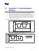
9.1 The I/O Domain Debug Port Guidelines
The recommended implementation is to have one debug port for each I/O domain. If a system does
not support dual domains, then there will normally be only one debug port in the I/O system. For
dual-domain systems, there will normally be two debug ports, one for each domain. Some of the
debug port signals are optional. They may require use or may be left unconnected, depending on
platform architecture.
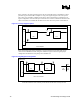
For either of these configurations, more than the minimum number of debug ports described above
may need to be implemented if signal integrity of the JTAG scan chains (particularly TCK) cannot
be met. This could occur if the platform partitions devices across several boards such that TCK
cannot be driven by the minimum number of debug ports and still provide clean clocks across the
board interfaces. Additional debug ports would be required to drive additional independent scan
chains in such cases.
Care must be taken to ensure that all JTAG signals of scan chains driven by each debug port are
used together for a set of devices. In particular, the TCK, TMS, TRST#, and TDI/TDO chains of
one debug port cannot be mixed with signals from another debug port. This is because each debug
port operates independently of the others.
Intel® E8870 chipset components were designed to support a 1.5 V pull-up voltage for the JTAG
signals. Simulations have shown that these processor inputs will function correctly with a VTP
pull-up of 1.2 V, but the system will have additional noise margin if the VTAP voltage is 1.5 V.
Some of the debug port signals are optional. They may require use or may be left unconnected,
depending on platform architecture. In particular:
• The DBA# signal will only be necessary if the target system requires selection between
alternate sources for control of the JTAG scan chains.
• The DBR# signal will only be necessary if there is a need to independently assert a local reset
to that sub-section of the system. Note that at least one DBR# should be implemented from
some debug port so that the ITP host can force a hardware reset of the platform.
• The FBI signal will only be necessary if there is a need to drive TCK via clock buffers to
devices in the local scan chain. TCK for the scan chain would normally be driven directly by
the debug port TCK output.