
ITP700 Debug Port Design Guide


R
72 ITP700 Debug Port Design Guide
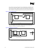
8.2.3 BPM Connectivity for I/O Domain Debug Ports
The Itanium 2 processor-based chipset has the capability to attach an ITP to the chipset
components within each IO Domain to provide debug hooks to the IO subsystem and Scalability
Port Switch components. IO Domain debug ports must follow the following guidelines:
• For single-domain systems, all SNCs, SPSs and IOHs should be connected to a single wired-
OR EV[3:0]# bus. This will support inter-device communication for performance and
debugging operations.
• For dual-domain systems, each SNC and IOH is gated by a bus coupler onto either a domain 0
or domain 1 wired-OR EV[3:0]# bus. Control of the bus couplers is normally driven by the
GPIO outputs from an SPS with the system configuration mode set to “connect” each device
to a bus. This allows the devices to be configured into a single common bus or into a bus for
each domain. Note that every SPS should be wired to the domain 0 EV[3:0]# bus, since only
the first domain for events is supported.
• An ITP debug port should be installed in each partitioned domain of the IO subsystem to
drive the local JTAG scan chain, sense the EV[3:0]# signals and possibly drive the EV[0]#
signal. BPM[4,0]# are not used, and must be routed to the “Common” Logic Analyzer
Connector as defined in the applicable Platform Design Guide.
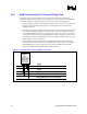
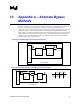
Figure 20. Intel
®
Itanium
®
2 IO Domain BPM Connectivity
Debug
Port
BPM5DR#
BPM[5]#
BPM[4]#
BPM[3]#
BPM[2]#
BPM[1]#
BPM[0]#
EV[3]#
EV[2]#
EV[1]#
EV[0]#
BPM[4]# Brought out to LA Connector
BPM[0]# Brought out to LA Connector