
ITP700 Debug Port Design Guide


R
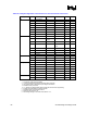
62 ITP700 Debug Port Design Guide
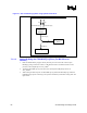
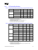
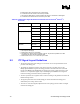
Figure 18 – ITP Clock Routing options using System Clock Driver
1K
1K
ITP Debug Port
Intel®
Pentium® 4
Processor
System Clock
Driver
BCLK[p:n]
ITPCLKOUT[0]
ITPCLKOUT[1]
ITPCLK[1:0]
2
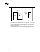
7.1.1.2 Option B) Using the ITPCLKOUT[1:0] Pins: (For B0 Silicon or
Greater)
1. Route the ITPCLKOUT[1:0] pins directly from the processor to the ITP connector pins
BCLK[n:p] using 33 Ω series resistors, 33 Ω pull-down source termination resistors at the
processor, and 1 kΩ pull-ups to VCC_CORE.
2
2. Terminate ITPCLKOUT[1:0] on the processor with separate1 kΩ pull-up resistors to
VCC_CORE.
1
3. When routing the ITP interposer to ITPCLKOUT[1:0] (instead of ITPCLK[1:0]), isolate the
ITPCLKOUT[1:0] from connecting to the system to eliminate system board routing stubs. See
figure below.