
ITP700 Debug Port Design Guide

R
30 ITP700 Debug Port Design Guide
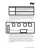
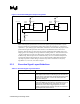
The debug port should be placed as close as is physically reasonable to the processor and no
further than 1.0 ns flight time (as measured by trace length of the BPM[5:0]#) from the processor.
System designers should record the flight time of the BPM[5:0]# signals from the processor to the
debug port. This value will be important during the routing of several other debug port signals.
Ideally BPM[5]# will be routed from the processor to the debug port BPM[5]# pin matched with
the other BPM# s. From pin 13 the trace will route directly to the debug port BPM5DR# pin and
continue to the termination of the transmission line.
Assuming BCLK(p/n) signals are routed from the system clock buffer to each of the synchronous
clock agents with a matched length, the copy of BCLK(p/n) from the system clock buffer to the
ITP debug port must have a flight time equal to the matched length of the other synchronous clock
agents plus the flight time of the BPM[5:0]# signals from the nearest bus agent to the debug port
noted above. This will ensure that the same BCLK to BPM[5:0]# phase relationship seen at the
closest system bus agent will be present at the debug port pins. BCLK trace lengths may be
adjusted to center the recovery of BPM[5:0]# and RESET# at the debug port within the ITP
receiver setup and hold window.
Multiple layer transitions of the BCLK, BPM, and TCK signals will compromise signal integrity.
An effort should be made to minimize the number of layer transitions for these signals. Try to keep
the BCLK, BPM, and TCK signals referenced to GND whenever possible. If layer transitions are
required, stitching vias should be included near ever every layer transition of the BCLK, BPM,
and TCK signals, even when not referencing the same voltage. This is recommended to reduce the
lengths of return current loops. Adding an AC bypass capacitor near every layer transition or plane
split between the two referenced planes will also help to minimize AC return current loops. An
effort should be made to not share ITP AC bypass capacitors with other high-speed signals.
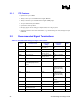
TCK and TMS have been successfully routed in a star topology with pull-up / pull-downs located
at the driver. FBO is routed such that it is connected to the TCK at the nearest system bus agent,
and routed back to the debug port with an electrical length equal to the flight time of the
BPM[5:0]# signals from the same system bus agent to the debug port. This is done to guarantee
that the BCLK to TCK phase relationship at the closest system bus agent will be seen at the debug
port FBO and BCLK(p/n) pins. The diagram below illustrates these routing relationships.