
Intel Xeon Processor and Intel E7500/E7501Chipset Compatible Platform Design Guide

Intel
®
Xeon™ Processor and Intel
®
E7500/E7501 Chipset Compatible Platform Design Guide 83
Memory Interface Routing Guidelines
Memory Interface Routing Guidelines 6
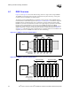
The E7500 chipset MCH and E7501 chipset MCH memory interface consist of two DDR memory
channels that operate in “lock-step.” Each channel consists of 64 data and eight ECC bits.
Logically, this is one, 144-bit wide memory bus; electrically, each channel is separate.
The E7501 chipset MCH supports an additional feature to the E7500 chipset MCH: DDR266. The
E7500 chipset MCH only supports DDR200 while the E7501 chipset MCH supports both DDR200
and DDR266. This chapter only documents the configurations Intel simulated to support these
features. The customer should simulate any deviations from these recommendations. A 2-DIMM
per-channel configuration may be used with the “3-DIMM Solution” recommendations.
This chapter covers routing guidelines for the DDR interfaces. Note that these guidelines apply to
both channel A and channel B. Each DDR interface has six signal types: Command Clocks, Source
Clocked Signals, Source Synchronous Signals, Chip Selects, Clock Enable, and DC Biasing. Refer
to the Intel
®
E7500 Chipset Memory Controller Hub (MCH) Datasheet and Intel
®
E7501 Chipset
Memory Controller Hub (MCH) Datasheet for details on the signals.
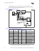
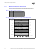
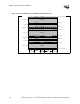
Table 6-1. DDR Channel Signal Groups
Group Signal
Source Synchronous Signals
DQS_x[17:0]
DQ_x[63:0]
CB_x[7:0]
Command Clocks
CMDCLK_x[3:0]
CMDCLK_x[3:0]#
Source Clocked Signals
MA_x[12:0]
RAS_x#
CAS_x#
WE_x#
BA_x[1:0]
Chip Selects CS_x[7:0]#
Clock Enable CKE_x
DC Biasing See Table 6-9