
ITP700 Debug Port Design Guide


R
ITP700 Debug Port Design Guide
87
14 Appendix E – Designer’s Checklist
for Schematic and Layout
Reviews
The following tables serve as a guide for a designer to review a generic ITP700 debug port
implementation in detail. These guidelines are in no means comprehensive nor serve to replace the
recommended design guidelines in this document.
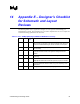
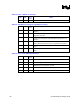
Table 41. Part 1: BPM[5:0]#BCLK(p/n) DBR# and RESET# Connectivity
Pas FAIL Don’t
Care
ISSUE
RESET# should be connected to the debug port (DP) pin15 and all front
side bus agents in a processor scan chain. I/O subspace scan chains may
connect to a suitable RESET# signal, but this connection is not required.
If RESET# is not used, proper pull-up is in place. This is required for ITP
S/W functionality.
BPM[5:0]# (DP pins 13, 11, 9, 7, 5, and 3 respectively) should be
connected to the BPM or other event signals according to best known
methods.
BPM5DR# must be connected to BPM5# at the DP (pins 23 and 13
respectively).
No other loads in a CPU Node ITP implementation are connected to the
BPM[5:0]# and RESET# traces other than processor, chipset, or DP loads.
DBR# is connected to an appropriate position in the reset generation logic.
Note that a DBR# reset should not result in any power sequencing on the
target system.
BCLK(p/n) polarity is correct. (BCLKp rising edge is a BCLK assertion)