
Intel Xeon Processor and Intel E7500/E7501Chipset Compatible Platform Design Guide

System Bus Routing Guidelines
72 Intel
®
Xeon™ Processor and Intel
®
E7500/E7501 Chipset Compatible Platform Design Guide
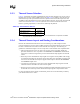
5.3.6.1 Voltage Translation for INIT#
A voltage translator circuit is required for the INIT# signal for all platforms that use the FWH. The
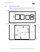
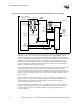
required routing topology for INIT# is given in Figure 5-8. Do not route a stub when routing to the
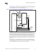
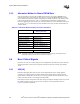
processors. Figure 5-9 shows the voltage translator circuit.
NOTE: The total trace length between the ICH3-S pin and the Processor 0 pin must be less than 15 inches.
NOTE: T1 and T2 must be referenced to ground.
Figure 5-8. INIT# Routing Topology
Intel
®
ICH3-S
Processor 0 Processor 1
0.1" – 3.0"
0.1" – 9.0"
VCC_CPU
200 Ω ± 5%
0.1" – 9.0"
0.1" – 9.0"
Voltage
Translator
FWH
Figure 5-9. Voltage Translator Circuit
From Driver
To Receiver
3904
3904
Vcc of Receiver
300 Ω
± 5%
470 Ω
± 5%
T1
T2
T1 = 10" max
T2 = 3" max
470 Ω
± 5%