
Intel Xeon Processor and Intel E7500/E7501Chipset Compatible Platform Design Guide

Intel
®
Xeon™ Processor and Intel
®
E7500/E7501 Chipset Compatible Platform Design Guide 49
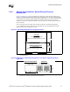
Platform Clock Routing Guidelines
NOTES:
1. The skew budget includes clock driver output pair to output pair jitter (differential jitter) and skew, clock skew
due to interconnect process variation, and static skew due to layout differences between clocks to all bus
agents.
2. This number does not include clock driver common mode (cycle to cycle) jitter or spread spectrum clocking.
3. The interconnect portion of the total budget for this specification assumes clock pairs are routed on a single
layer and routed no longer than the maximum recommended lengths.
4. Skew measured at the load between any two-bus agents. Measured at the crossing point.
5. Edge to edge spacing between the two traces of any differential pair. Uniform spacing should be maintained
along the entire length of the trace.
6. Clock traces are routed in a differential configuration. Maintain the minimum recommended spacing between
the two traces of the pair. Do not exceed the maximum trace spacing because this degrades the noise
rejection of the network.
7. Set line width to meet correct motherboard impedance. The line width value provided here is a
recommendation to meet the proper trace impedance based on the recommended stack-up.
8. The differential impedance of each clock pair is approximately 2*Zsingle-ended*(1-2*Kb) where Kb is the
backwards cross-talk coefficient. For the recommended trace spacing, Kb is very small, and the effective
differential impedance is approximately equal to 2 times the single-ended impedance of each half of the pair.
9. The single ended impedance of both halves of a differential pair should be targeted to be of equal value. They
should have the same physical construction. If the HOST_CLK traces vary within the tolerances specified,
both traces of a differential pair must vary equally.
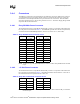
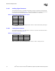
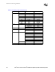
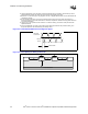
Table 4-3. HOST_CLK[1:0]# Routing Guidelines
Layout Guideline Value Reference Notes
HOST_CLK Skew between Agents
300 ps total budget:
150 ps for clock driver
150 ps for interconnect
Figure 4-3 1,2,3,4
Trace Width 5 mils Figure 4-4 7
Differential Pair Spacing 20 – 25 mils Figure 4-4 5,6
Spacing to Other Traces 25 mils Figure 4-4
Serpentine Spacing
Maintain a minimum S1/h ratio of
> 26/5
Section 12.3
Motherboard Impedance – Differential 100
Ω typical 8
Motherboard Impedance – Single Ended 50
Ω ± 10% 9
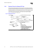
Processor, ITP and MCH Routing Length –
L1, L1’: Clock Driver to Rs
0 – 0.5” Figure 4-2 11
Processor, ITP and MCH Routing Length –
L2, L2’: Rs to Rs-Rt Node
0 – 0.2” Figure 4-2 11
Processor, ITP and MCH Routing Length –
L3, L3’: Rs-Rt Node to Rt
0 – 0.2” Figure 4-2 11
Processor, ITP and MCH Routing Length –
L4, L4’: Rs-Rt Node to Load
0 – 20” Figure 4-2 12
Processor to MCH Length Matching (LT)
0.044” ± 0.025”
MCH LT must be 0.044” shorter
than processor LT.
Figure 4-2 10
Processor to Processor Length Matching (LT)
± 25 mils Figure 4-2 13
Processor to ITP Length Matching (LT) See ITP700 Port Design Guide Figure 4-2 14
HOST_CLKn – HOST_CLKn# Differential
Pair Length Matching
± 25 mils
Rs Series Termination Value 20 – 33
Ω ± 5% Figure 4-2
Rt Shunt Termination Value
49.9
Ω ± 1%
(for 50
Ω board impedance)
Figure 4-2