
ITP700 Debug Port Design Guide


R
ITP700 Debug Port Design Guide 31
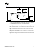
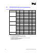
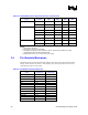
Figure 8. Recommended Layout Topology
Debug Port
System Bus
Agent
System Bus
Agent
System Bus
Agent
System Bus
Agent
System
Clock
Driver
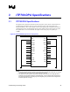
27 Ohms
T
0
T
1
(T
1
+T
BPM
)
(T
0
+T
BPM
)
(T
TCK
+T
BPM
)
T
TCK
FBO
BPMn
BCLK
TCK
TCK TCK
TCK TCK
BPMn
BCLK BCLK
BCLKBCLK
T
0
T
0
T
0
T
TCK
T
TCK
T
TCK
NOTES:
1. All of the above routes must be simulated to ensure signal integrity. Failure to do so may result in non-
functional ITP.
2. All combination timings in the above drawing are ± 50 ps in routing length maximum.
The figure above defines propagation delays of various ITP signals from the driver to the receiver.
The following are definitions of individual trace segments that are included in the figure.
• T
TCK
– Propagation delay of the TCK trace from the debug port to the system bus agent TCK
pin
• T
BPM
– Propagation delay of the BPM traces from the debug port to the nearest system bus
agent.
• T
0
– Propagation delay of BCLK from the system clock driver to the processors and chipset
Components
• T
1
– Propagation delay of the BPM traces from the driving system bus agent to the system bus
agent closest to the debug port.