
Intel Xeon Processor and Intel E7500/E7501Chipset Compatible Platform Design Guide

Platform Power Delivery Guidelines
200 Intel
®
Xeon™ Processor and Intel
®
E7500/E7501 Chipset Compatible Platform Design Guide
When analyzing systems that may be “marginally compliant” to the 2 V Rule, attention must be
paid to the behavior of the ICH3-S’s RSMRST# and PWROK signals because they control internal
isolation logic between the various power planes:
• RSMRST# controls isolation between the RTC well and the resume wells.
• PWROK controls isolation between the resume wells and main wells.
If one of these signals goes high while one of its associated power planes is active and the other is
not, a leakage path will exist between the active and inactive power wells. This could result in high,
possibly damaging, internal currents.
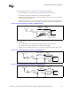
The circuit in Figure 11-26 may, under high temperature and parameter corner conditions, inject
charge onto the 1.8 V rail at steady state. The circuit in Figure 11-25 does not have this
characteristic; however, it is more susceptible to layout variations and should be fully analyzed and
tested to make sure that the implementation meets the 2 V specification. When choosing between
the two circuits a designer should understand the trade-offs with respect to their linear regulator
design and application.
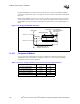
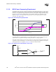
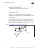
The Semtech SC4431 monitors the difference between the reference pin (from 3.3 V) and the
ground pin (1.8 V). The SC4431 turns on its output when the difference between 1.8 V and 3.3 V is
over 1.9 V. Connecting the SC4431 ground pin to 1.8 V requires a series resistor from 1.8 V to
ground to complete the current path from the SC4431 VCC (5 VSB) to system ground. The series
resistor must be able to dissipate 0.25 W. This can be achieved using a 25
Ω resistor in a 1206
package, or two 51
Ω resistors in 0805 packages. The 1.8 V rail should be able to sink the current
from the SC4431 and the 1.13 k
Ω / 2.05 kΩ divider.
NOTE: This circuit has not yet been validated. Resistor values are subject to change.
Figure 11-26. Another Example 1.8 V/3.3 V Power Sequencing Circuit
3.3 V
VCC
GND
OUT
REF
1.8 V
5 VSB
2.05 kΩ 1%
1.13 kΩ 1%
10 Ω
Semtech
SC4431
0 Ω
NOPOP
1 µF
NOPOP
51 Ω
0805
51 Ω
0805