
Intel Xeon Processor and Intel E7500/E7501Chipset Compatible Platform Design Guide

Intel
®
Xeon™ Processor and Intel
®
E7500/E7501 Chipset Compatible Platform Design Guide 135
Intel
®
82870P2 (P64H2)
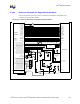
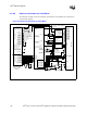
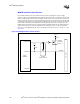
8.2.7.9 Reference Schematic for Dual-Slot Parallel Mode
Note that the following schematic is based on definition and simulation of the P64H2. This
schematic has not been fully validated.
Figure 8-19. Reference Schematic for Dual-Slot Parallel Mode
PCIXCAP
M66EN
SLOT 1 Present 1
SLOT 1 Present 2
--12V
+12V
+5V
+3V
--12V
+12V
+5V
+3V
Fault#
Pwren 1
RST #
CLK
Power
Logic
PxAD[63:0]
PxC/BE[7:0]
PxPAR
PxPAR64
PxREQ64#
PxACK64#
PxFRAME#
PxIRDY#
PxTRDY#
PxSTOP#
PxDEVSEL#
PxPLOCK#
PxGNT0#
PxPERR#
PxSERR#
PxREQ0#
PCI SLOT 1
15K
3.3V
Intel
®
P64H2
PxPCLKO [0]
PxPCLKI
PxAD[63:0]
PxC/BE[7:0]
PxPAR
PxPAR64
PxREQ64#
PxACK64#
PxFRAME#
PxIRDY#
PxTRDY#
PxSTOP#
PxDEVSEL#
PxPLOCK#
PxGNT[0]#
PxPERR#
PxSERR#
PxREQ[0]#
PxM66EN
PxPCIXCAP
PxIRQ[15] (HxSWITCHA)
PxIRQ[14] (HxFAULTA#)
PxIRQ[13] (HxPRSNT2A)
PxIRQ[12] (HxPRSNT1A)
PxIRQ[11] (HxM66ENA)
HPxSLOT[2] (HXPCIXCAP1A)
HPxSLOT[1] (HXPCIXCAP2A)
PxGNT[5]# (HxRESETA#)
HPxSOC (HxGNLEDA)
HPxSOL (HxAMLEDA)
HPxSORR# (HxBUSENA#)
HPxSIL# (HxCLKENA#)
HPxSOD (HxPWRENA)
PxIRQ[10] (HxSWITCHB)
PxIRQ[9] (HxFAULTB#)
PxIRQ[8] (HxPRSNT2B)
PxREQ[5] (HxPRS NT1B)
PxREQ[4] (HxM66ENB)
PxREQ[3] (HXPCIXCAP1B)
HPxSLO T[0] (HXPCIXCAP2B)
HPxSOR# (HxRESETB#)
HPxSIC (HxGNLEDNB)
HPxSID (HxAMLEDB)
PxGNT[4] (HxBUSENB#)
PxGNT[3] (HxCLKENB#)
HPxSOLR (HxPW RENB)
330
Switch
330
33
33
ENB
PWROK
PxPCLKO [6]
PxREQ[2]#
should be pulled
to 3.3V through
8.2K
8.2K
3.3V
PCIXCAP
M66EN
SLOT 1 Present 1
SLOT 1 Present 2
--12V
+12V
+5V
+3V
RST #
CLK
PxAD[63:0]
PxC/BE[7:0]
PxPAR
PxPAR64
PxREQ64#
PxACK64#
PxFRAME#
PxIRDY#
PxTRDY#
PxSTOP#
PxDEVSEL#
PxPLOCK#
PxGNT1#
PxPERR#
PxSERR#
PxREQ0#
PCI SLOT 2
PxPCLKO [1]
33
--12V
+12V
+5V
+3V
Fault#
Pwren 1
Power
Logic
Busen#
PCI BUS SIGNALS
PCI BUS SIGNALS
Slot 1 Bus
Switch
Busen#
PCI BUS SIGNALS
PCI BUS SIGNALS
Slot 2 Bus
Switch
Clken#
PxPCLKO 0
PxPCLKO 0
Slot 1 Clock
Switch
Clken#
PxPCLKO 1
PxPCLKO 1
Slot 1 Clock
Switch
10K
2.2K
10K
8.2K
3.3V
8.2K
3.3V
3.3V
5.6K
10K
3.3V
Comparator
Comparator
3.3V
10K
2.2K
10K
8.2K
3.3V
8.2K
3.3V
5.6K
10K
3.3V
Comparator
Comparator
3.3V
3.3V
1K
15K
3.3V
330
Switch
330
PxGNT[1]#
PxREQ[1]#
10K
10K
Input to PWROK
10K
10K
3.3V
Inverter
ENB
3.3V
Note * All PCI signals muxed or not need to follow PCI spec 2.2 pullup requirements
4:2
MUX
SEL
S1
S2
S3
S4
D1
D2
Truth Table
SEL D1 D2
0 S1 S2
1 S3 S4
85
85
85
85
PxM66EN needs to
be routed to each
PCI Slot by means
of a bus switch so
that the P64H2 can
drive this signal
when appropriate
15K
3.3V
PxM66EN
100K
10K
3.3V
5K
3.3V
5K
5K
3.3V
5K