
Voltage Regulator Module (VRM) and Enterprise Voltage Regulator-Down (EVRD) 10.1 Design Guidelines

Voltage Regulator Module (VRM) and Enterprise Voltage 19
Regulator-Down (EVRD) 10.1 Design Guidelines
3 Control Signals
3.1 Output Enable (OUTEN) - REQUIRED
The VRM/EVRD should accept an input signal to enable its output voltage. When disabled, the
regulator’s output should go to a high impedance state and should not sink or source current. When
OUTEN is pulled low during the shutdown process, the VRM/EVRD should not exceed the
previous voltage level regardless of the VID setting during the shutdown process. Once operating
after power-up, it should respond to a deasserted OUTEN within 500 ms. The circuitry driving
OUTEN is an open-collector/drain signal. It is EXPECTED that the pull-up resistor will be
located on the baseboard and will not be integrated into the PWM controller chip or VRM.
3.2 Voltage Identification (VID [5:0]) - REQUIRED
VID [4:0] are compatible with Intel
®
Pentium
®
4, Intel
®
Xeon™ processors, and Intel
®
Xeon™
processor MP using 5-bit VID codes. VID [5] will be used on the next generation of processors
with 6-bit VID codes.
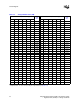
The VRM/EVRD must accept six lines to set the nominal voltage as defined by Table 3-3. When
the VID [4:0] inputs are all high (in this case VID5 is a don’t care), such as when no processor is
installed, the regulator should disable its output voltage. If this disable code appears during
previously normal operation, the regulator should turn off its output within 500 ms. The circuitry
driving VID [5:0] is an open-collector/drain signal. It is EXPECTED that the pull-up resistors will
be located on the baseboard and will not be integrated into the PWM controller chip or VRM.
Other platform components may use VID inputs and may require tighter limits than specified in
Table 3-2.
A normal no-processor VID [5:0] code for a Vcc regulator will be X11111, where X is defined as
logic 1 or 0, disabling the VRM/EVRD.
NOTE:
1. Other platform components may use VID inputs and may require tighter limits.
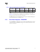
Table 3-1. OUTEN Specifications
Symbol Parameter Min Max Units
VIH Input Voltage High 0.8 3.465 V
VIL Input Voltage Low 0 0.4 V
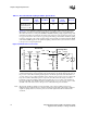
Table 3-2. VID [5:0] Specifications
Symbol Parameter Min Max Units Notes
V
IH
Input High Voltage 0.8 3.465 V 1
V
IL
Input Low Voltage 0 0.4 V 1