
Voltage Regulator Module (VRM) and Enterprise Voltage Regulator-Down (EVRD) 10.1 Design Guidelines

Output Voltage Requirements
10 Voltage Regulator Module (VRM) and Enterprise Voltage
Regulator-Down (EVRD) 10.1 Design Guidelines
The continuous load current can also be referred to as the Thermal Design Current (TDC). TDC is
the sustained (DC equivalent) current that the processor is capable of drawing indefinitely and
defines the current to use for the voltage regulator temperature assessment. At TDC, switching
FETs reach maximum allowed temperature and may heat the baseboard layers and neighboring
components. The envelope of the system operating conditions establishes actual component and
baseboard temperatures. This includes voltage regulator layout, processor fan selection, ambient
temperature, chassis configuration, etc. To avoid heat related failures, baseboards should be
validated for thermal compliance under the envelope of system operating conditions. It is proposed
that the voltage regulator thermal protection be implemented for all designs
(Section 6.2).
The max load current represents the maximum peak current that the processor is capable of
drawing. It is the maximum current the VRM/EVRD must be electrically designed to support
without tripping any protection circuitry.
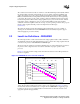
2.2 Load Line Definitions - REQUIRED
The following load line contains static and transient voltage regulation data as well as maximum
and minimum voltage levels. The differential remote sense points for the voltage regulator must be
connected to the processor VCCSENSE and VSSSENSE pins.
The upper and lower load lines represent the allowable range of voltages that must be presented to
the processor. The voltage must never exceed these boundaries for proper operation of the
processor.
Figure 2-2 shows the load line voltage offsets and current levels based on the VID specifications
for the core regulator.
The encoding in Table 2-1 for the load lines is valid for the range of load current from 0 A to
120 A. The Load Line 0 (LL0) and Load Line 1 (LL1) control signals from Section 3.4, form a
2-bit load line selection and will be used to configure the Vcc VRM/EVRD to supply the proper
load lines for the processor. For implementation of LL0 and LL1 on the baseboard refer to the
appropriate platform design guidelines.
Figure 2-2. VRM/EVRD 10.1 Processor Die Load Line
-0.200
-0.180
-0.160
-0.140
-0.120
-0.100
-0.080
-0.060
-0.040
-0.020
0.000
0 20 40 60 80 100 120
Icc (A)
Vcc (V) (Offset from VID)
Vmax
Vmin