
Voltage Regulator Module (VRM) and Enterprise Voltage Regulator-Down (EVRD) 10.0 Design Guidelines


VRM and EVRD 10.0 Design Guidelines
R
4
8.1
Operating Temperature PROPOSED ........................................................ 32
8.2
VRM Board Temperature REQUIRED....................................................... 32
8.3
Non-Operating Temperature PROPOSED ................................................ 32
8.4
Humidity PROPOSED................................................................................ 32
8.5
Altitude PROPOSED.................................................................................. 32
8.6
Electrostatic Discharge PROPOSED.........................................................33
8.7
Shock and Vibration PROPOSED .............................................................33
8.8
Electromagnetic Compatibility PROPOSED .............................................. 33
8.9
Reliability PROPOSED .............................................................................. 33
8.10
Safety PROPOSED....................................................................................33
9
Manufacturing Considerations ................................................................................ 34
9.1
Lead Free (Pb Free)................................................................................... 34
Figures
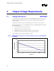
Figure 1. VRM/EVRD 10.0 Load Current vs. Time for Intel® Xeon™ Processor with 800
MHz System Bus .......................................................................................................10
Figure 2 VRM/EVRD 10.0 Load Current vs. Time for Low Voltage Intel® Xeon™
Processor with 800 MHz System Bus ....................................................................... 11
Figure 3. VRM/EVRD 10.0 Die Load Line .......................................................................12
Figure 4. Vcc Overshoot Example Waveform.................................................................. 13
Figure 5. Power-On Sequence Block Diagram................................................................ 14
Figure 6. Power-On Sequence Timing Diagram..............................................................14
Figure 7. Processor Transition States .............................................................................15
Figure 8. Example Processor VID Transition States .......................................................16
Figure 9. Model of Processor Load.................................................................................. 17
Figure 10. VRM 10.0 Module and Connector .................................................................. 31
Tables
Table 1. Icc Guidelines ....................................................................................................12
Table 2. Capacitor Recommendations ............................................................................17
Table 3. OUTEN Specifications ....................................................................................... 18
Table 4. VID Specifications.............................................................................................. 18
Table 5. Voltage Identification (VID) ................................................................................ 19
Table 6. VRM_pres# Specifications.................................................................................20
Table 7. Vcc_PWRGD Specifications.............................................................................. 26
Table 8. VR_hot# Specifications......................................................................................26
Table 9. VRM 10.0 Connector Vendor and Part Numbers .............................................. 28
Table 10. VRM 10.0 Connector Pin Descriptions ............................................................ 29
Table 11. VRM Pins ......................................................................................................... 30