
Voltage Regulator Module (VRM) and Enterprise Voltage Regulator-Down (EVRD) 10.0 Design Guidelines

VRM and EVRD 10.0 Design Guidelines
R
16
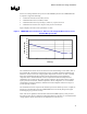
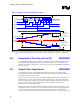
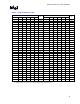
Figure 8. Example Processor VID Transition States
high VID to low VID
Vcc transition
450 mV
50 µs maximum settling
from registering final VID
450 mV
low VID to high VID
Vcc transition
VID 5
36 VID steps @ 5 µs each step = 180 µs
Upper equals
Final VID-1.25mΩ*Icc
Lower equals
Start VID-1.25mΩ*Icc - 40mV
Maximum
Vcc
settling
Upper equals
Start VID-1.25mΩ∗Icc
Lower equals
Final VID-1.25mΩ*Icc - 40mV
50 µs maximum settling
from registering final VID
VID 4
VID 3
VID 2
VID 1
VID 0
400 ns
worst case VID
settling time
NOTE: For ease of illustration, the diagram assumes steady state, constant current during the dynamic VID Transition. Actual
processor behavior allows for any dlcc/dt event during the transitions, depending on the code it is executing at that
time.
2.8 Overshoot at Turn-On or Turn-Off REQUIRED
The VRM/EVRD output voltage should remain within the load-line regulation band for the VID
setting while the VRM/EVRD is turning on or turning off, with no over- or undershoot out of
regulation. No negative voltage below –100 mV may be present at the VRM/EVRD output during
turn-on or turn-off.
2.9 Output Filter Capacitance REQUIRED
The output filter capacitance for VRM based designs will be located on the baseboard. The
system design must ensure that the output voltage of the VR conforms to the load line of Figure 3
with the baseboard and processor loads.
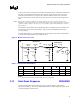
Figure 9 is a representative example of a baseboard decoupling solution and a processor load. The
values shown are for a four–phase switching voltage regulator design . The parasitic baseboard
values are extracted from a design using a four-layer baseboard with 2 ounces total of copper for
Vcc and 2 ounces total of copper for ground. The amount of bulk decoupling required is
dependent on the voltage regulator design.
This design incorporates at least ten 560 µF Aluminum-polymer bulk capacitors and forty 10 µF
ceramic high frequency capacitors per processor (Table 2). Eight of the 10 µF capacitors should
be placed in the cavity of the processor socket. The remaining 32 capacitors should be split
evenly such that half are on one side of the processor socket and half are on the other side as close