
Intel Xeon Processor and Intel E7500/E7501Chipset Compatible Platform Design Guide

Memory Interface Routing Guidelines
84 Intel
®
Xeon™ Processor and Intel
®
E7500/E7501 Chipset Compatible Platform Design Guide
6.1 DDR Overview
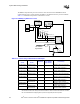
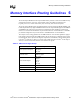
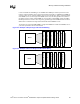
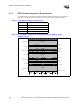
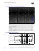
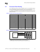
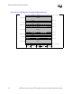
Figure 6-1 and Figure 6-2 show both channels being routed to a single “bank” of eight DIMMs.
The DIMMs are physically interleaved. Intel recommends using this interleaving, starting with
Channel B closest to the MCH, for optimal routing.
The platform requires DDR DIMMs to be populated in-order, starting with the DIMMs furthest
from the MCH in a “fill-farthest” approach (see Figure 6-1 and Figure 6-2). In addition, single rank
DIMMs should be populated furthest when a combination of single ranked and double ranked
DIMMs are used. This recommendation is based on the signal integrity requirements of the DDR
interface. Intel’s recommendation is to check for correct DIMM placement during BIOS
initialization. Additionally, it is strongly recommended that all designs follow the DIMM ordering,
SMBus Addressing, Command Clock routing and Chip Select routing documented in Figure 6-1
and Figure 6-2. This addressing must be maintained to be compliant with the reference BIOS code
supplied by Intel. For a 2-DIMM board, follow the same methodology.
Figure 6-1. 3-DIMM per-Channel Implementation
Figure 6-2. 4-DIMM per-Channel Implementation
MCH
D
I
M
M
A3
02h
2/2#
4/5
D
I
M
M
B3
06h
2/2#
4/5
D
I
M
M
A2
01h
1/1#
2/3
D
I
M
M
B2
05h
1/1#
2/3
D
I
M
M
A1
00h
0/0#
0/1
D
I
M
M
B1
04h
0/0#
0/1
Fill Third
Fill Second Fill First
SMBus Address:
Command Clock:
Chip Select:
Single Rank DIMMs
Dual Rank DIMMs
MCH
D
I
M
M
A4
03h
3/3#
6/7
D
I
M
M
B4
07h
3/3#
6/7
D
I
M
M
A3
02h
2/2#
4/5
D
I
M
M
B3
06h
2/2#
4/5
D
I
M
M
A2
01h
1/1#
2/3
D
I
M
M
B2
05h
1/1#
2/3
D
I
M
M
A1
00h
0/0#
0/1
D
I
M
M
B1
04h
0/0#
0/1
Fill Fourth Fill Third Fill Second Fill First
SMBus Address:
Command Clock:
Chip Select:
Single Rank DIMMs
Dual Rank DIMMs