
603 Pin Socket Design Guidelines

603 Pin Socket Design Guidelines
R
13
actuation must meet or exceed SEMI S8-95 Safety Guidelines for Ergonomics/Human Factors
Engineering of Semiconductor Manufacturing Equipment, example Table R2-7 (Maximum Grip Forces)
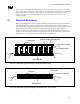
3.5.3. Visual Aids:
The socket top will have markings identifying open and closed positions for the handle.
The socket top will have markings identifying Pin 1. This marking will be represented by a triangular
symbol. See Figure 9-5 (Appendix A.5).
3.5.4. Equipment Pick and Place:
The preferred method to transfer surface mount connectors from the packaging media to the board
assembly is to use a vacuum actuated nozzle. Vacuum cup area on the connector needs to be available
to securely hold the part during transfer and placement. Considerations for the size of the area include
connector mass, mass symmetry, acceleration/deceleration transfer rate, angular momentum, and
location precision of the connector in the packaging media. Typically, a 10mm diameter vacuum nozzle
can support a maximum load of 15g.
3.5.5. Solderability Test:
Must pass 95% coverage per solder ball/surface mount feature.
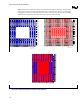
3.5.6. Socket BGA Co-Planarity:
The co-planarity requirement for all solderballs or surface mount features on the underside of the socket
is defined as follows.
Solder balls must have a co-planarity of 0.20mm maximum over the entire ball field.
Leads must have a co-planarity of 0.15mm maximum over the entire field.
3.5.7. Solder Ball/Surface Mount Feature True Position:
The solder balls/surface mount features have a 0.41mm true position requirement with respect to Datum
A, B, and C see Figure 9-5 (Appendix A.5).
3.6. Assembly Requirements to the Motherboard:
3.6.1. Surface Mountable:
The socket must be a surface mount socket design and able to mount to pads and VIP.
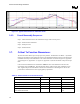
3.6.2. Reflow Characteristics:
Max Temperature: 240°C