
VRM 9.1 DC-DC Converter Design Guidelines
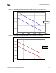
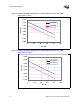
Table Of Contents
- 1 Electrical Specifications
- 1.1 Output Requirements
- 1.1.1 Voltage and Current - REQUIRED
- 1.1.2 Maximum Ratings - EXPECTED
- 1.1.3 Output Voltage Tolerance - REQUIRED
- 1.1.4 No-Load Operation - REQUIRED
- 1.1.5 Turn-on Response Time - EXPECTED
- 1.1.6 Overshoot and Undershoot at Turn-On or Turn-Off - REQUIRED
- 1.1.7 Converter Stability - REQUIRED
- 1.1.8 Current Sharing - REQUIRED
- 1.2 Input Voltage and Current
- 1.3 Control Inputs - REQUIRED
- 1.4 Remote Sense (VO-sen+, VO-sen-) - EXPECTED
- 1.5 Power Good Output (PWRGD) - REQUIRED
- 1.6 VRM Present (VRM-pres) - EXPECTED
- 1.7 Efficiency - PROPOSED
- 1.8 Isolation - PROPOSED
- 1.9 Fault Protection
- 1.1 Output Requirements
- 2 Module Layout Guidelines
- 3 Environmental Conditions
- 3.1 Operating Temperature - PROPOSED
- 3.2 VRM Board Temperature - REQUIRED
- 3.3 Non-Operating Temperature - PROPOSED
- 3.4 Humidity - PROPOSED
- 3.5 Altitude - PROPOSED
- 3.6 Electrostatic Discharge - PROPOSED
- 3.7 Shock and Vibration - PROPOSED
- 3.8 Electromagnetic Compatibility - PROPOSED
- 3.9 Reliability - PROPOSED
- 3.10 Safety - PROPOSED

Electrical Specifications
8 VRM 9.1 DC-DC Converter Design Guidelines
1.1.3 Output Voltage Tolerance - REQUIRED
The remote sense lines of each VRM should be routed on the system board to a remote sense point
at the geometric center of the processors, where they are connected to each other and to the Vcc
and Vss planes for Intel Xeon processors using the 603 socket. For 64-bit Intel Xeon processor MP
cache remote sense traces, the processor V
CCSENSE
and V
SSSENSE
pins should be connected to test
points on the baseboard in order to probe the die voltage. Unstuffed resistor pads on the baseboard
can be used for this purpose.
The VRM regulates this point as follows:
• VvrmMIN = 0.980 * VID_Setpoint_Voltage - VRM_Output_Current * 0.95 mΩ
• VvrmMAX = VID_Setpoint_Voltage - VRM_Output_Current * 0.95 mΩ
• Vvrm
MIN
and Vvrm
MAX
are VRM voltage regulation requirements measured at the power
plane reference point (VRM remote-sense star connection at the geometric center of the
processor loads on the system board).
• Vvrm
MIN
is the minimum voltage allowed for a given VRM output current.
• Vvrm
MAX
is the maximum voltage allowed for a given VRM output current.
See example load lines in Figure 1-1, Figure 1-2, Figure 1-3, and Figure 1-4 and their
corresponding numerical values in Table 1-2 and Table 1-3. The VRM shall regulate as defined
above for all VID set-points (except during input voltage turn-on and turn-off - see Section 1.1.6
for turn-on and turn-off tolerances).
Voltage tolerance includes:
• Initial DC output voltage set-point error
• Component aging effects
• Output ripple and noise from DC to 100 MHz
• Full ambient temperature range and warm up
• Static operation
• Dynamic output load changes
• Input voltage variations