
VRM 9.1 DC-DC Converter Design Guidelines
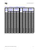
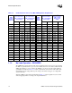
Table Of Contents
- 1 Electrical Specifications
- 1.1 Output Requirements
- 1.1.1 Voltage and Current - REQUIRED
- 1.1.2 Maximum Ratings - EXPECTED
- 1.1.3 Output Voltage Tolerance - REQUIRED
- 1.1.4 No-Load Operation - REQUIRED
- 1.1.5 Turn-on Response Time - EXPECTED
- 1.1.6 Overshoot and Undershoot at Turn-On or Turn-Off - REQUIRED
- 1.1.7 Converter Stability - REQUIRED
- 1.1.8 Current Sharing - REQUIRED
- 1.2 Input Voltage and Current
- 1.3 Control Inputs - REQUIRED
- 1.4 Remote Sense (VO-sen+, VO-sen-) - EXPECTED
- 1.5 Power Good Output (PWRGD) - REQUIRED
- 1.6 VRM Present (VRM-pres) - EXPECTED
- 1.7 Efficiency - PROPOSED
- 1.8 Isolation - PROPOSED
- 1.9 Fault Protection
- 1.1 Output Requirements
- 2 Module Layout Guidelines
- 3 Environmental Conditions
- 3.1 Operating Temperature - PROPOSED
- 3.2 VRM Board Temperature - REQUIRED
- 3.3 Non-Operating Temperature - PROPOSED
- 3.4 Humidity - PROPOSED
- 3.5 Altitude - PROPOSED
- 3.6 Electrostatic Discharge - PROPOSED
- 3.7 Shock and Vibration - PROPOSED
- 3.8 Electromagnetic Compatibility - PROPOSED
- 3.9 Reliability - PROPOSED
- 3.10 Safety - PROPOSED
VRM 9.1 DC-DC Converter Design Guidelines 15
Electrical Specifications
When disabled, the VRM should sink less than 100 mA from the 12 V Input and less than 1 A from
shared VRMs that remain on.
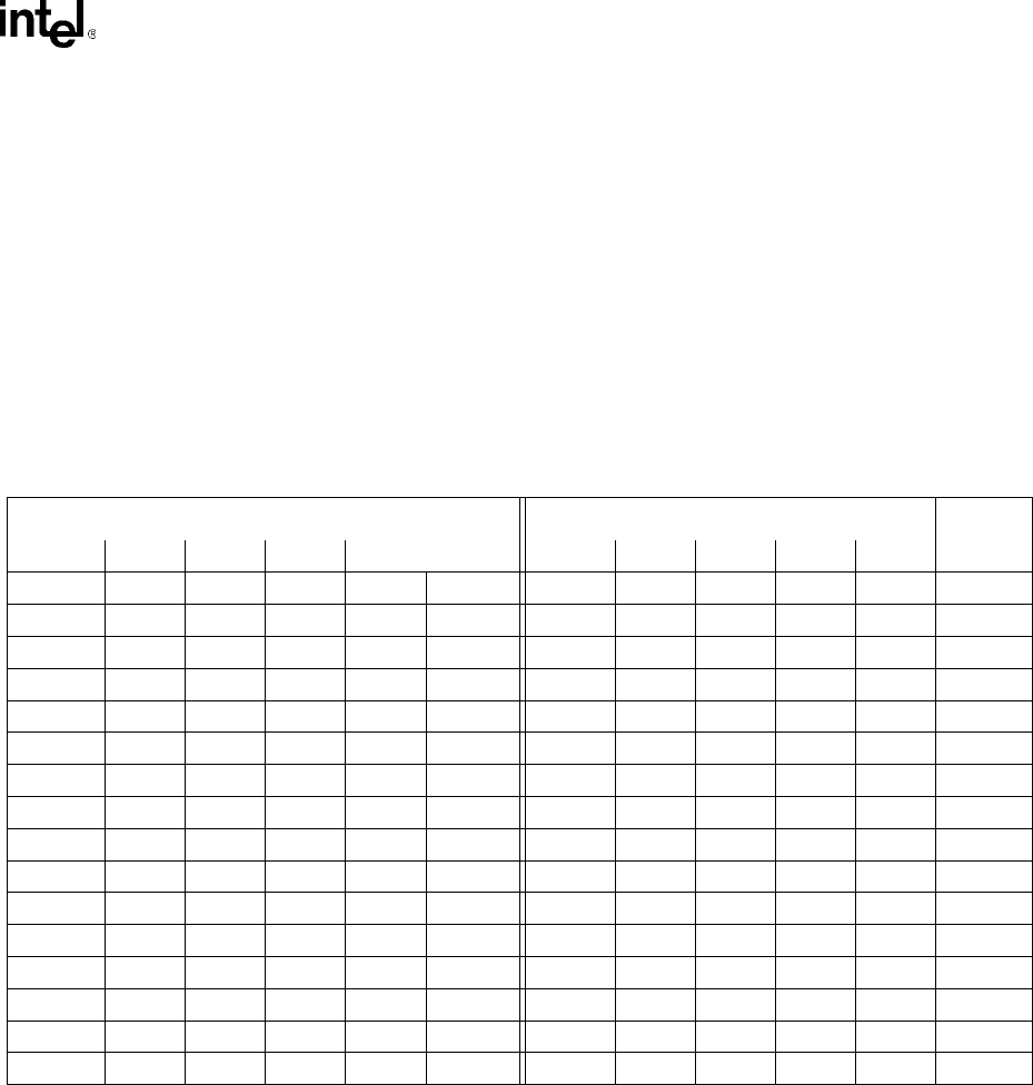
1.3.2 Voltage Identification—(VID[4:0]) - REQUIRED
The VRM must accept five lines to set the nominal (maximum) voltage as defined by the table
below. Five processor package pins will have a high-low pattern corresponding to the voltage
required by the individual processor. When all five VID inputs are high (11111), the VRM should
disable its output.
The maximum low-input voltage is 0.8V; the minimum high-input voltage is 1.7 V. Each VID
input should have a 1 kΩ ± 10% pull-up resistor to 3.3V ± 5%.
NOTE: When using the VRM as a cache regulator, only VID [3:0] will be utilized. VID4 should be pull up high as described in
section Voltage Identification—(VID[4:0]) - REQUIRED.
1.4 Remote Sense (VO-sen+, VO-sen–) - EXPECTED
A star remote sense connection should be provided at the geometric center of the processors to
allow the VRM to sense voltage and compensate for an output voltage offset of 55 mV in the
power distribution path. VO-sen+ is the + sense line, and VO–sen– is the sense return. Differential
sense inputs are required. In the event of an open sense line the VRM should maintain regulation
through a local sense resistor on the VRM board. Systems that do not use remote sense will not
connect these lines on the system board. The remote sense lines should draw no more than 10 mA,
to minimize offset errors.
Table 1-4. Voltage Identification (VID)
Processor Pins (0 = low, 1 = high)
Vcc
(V)
Processor Pins (0 = low, 1 = high)
Vcc
(V)
VID4
1
VID3 VID2 VID1 VID0 VID4
1
VID3 VID2 VID1 VID0
1 1111Off 0 11111.475
1 11101.1 0 11101.5
1 11011.1250 11011.525
1 11001.150 11001.55
1 10111.1750 10111.575
1 10101.2 0 10101.6
1 10011.2250 10011.625
1 10001.2500 10001.65
1 01111.2750 01111.675
1 01101.3 0 01101.7
1 01011.3250 01011.725
1 01001.350 01001.75
1 00111.3750 00111.775
1 00101.4 0 00101.8
1 00011.4250 00011.825
1 00001.450 00001.85