
VRM 9.1 DC-DC Converter Design Guidelines
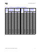
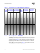
Table Of Contents
- 1 Electrical Specifications
- 1.1 Output Requirements
- 1.1.1 Voltage and Current - REQUIRED
- 1.1.2 Maximum Ratings - EXPECTED
- 1.1.3 Output Voltage Tolerance - REQUIRED
- 1.1.4 No-Load Operation - REQUIRED
- 1.1.5 Turn-on Response Time - EXPECTED
- 1.1.6 Overshoot and Undershoot at Turn-On or Turn-Off - REQUIRED
- 1.1.7 Converter Stability - REQUIRED
- 1.1.8 Current Sharing - REQUIRED
- 1.2 Input Voltage and Current
- 1.3 Control Inputs - REQUIRED
- 1.4 Remote Sense (VO-sen+, VO-sen-) - EXPECTED
- 1.5 Power Good Output (PWRGD) - REQUIRED
- 1.6 VRM Present (VRM-pres) - EXPECTED
- 1.7 Efficiency - PROPOSED
- 1.8 Isolation - PROPOSED
- 1.9 Fault Protection
- 1.1 Output Requirements
- 2 Module Layout Guidelines
- 3 Environmental Conditions
- 3.1 Operating Temperature - PROPOSED
- 3.2 VRM Board Temperature - REQUIRED
- 3.3 Non-Operating Temperature - PROPOSED
- 3.4 Humidity - PROPOSED
- 3.5 Altitude - PROPOSED
- 3.6 Electrostatic Discharge - PROPOSED
- 3.7 Shock and Vibration - PROPOSED
- 3.8 Electromagnetic Compatibility - PROPOSED
- 3.9 Reliability - PROPOSED
- 3.10 Safety - PROPOSED

Electrical Specifications
14 VRM 9.1 DC-DC Converter Design Guidelines
1.1.8.3 Negative Current Limit - EXPECTED
Because the output of the VRM will be connected in parallel with other voltage sources (other
VRMs) the VRM should incorporate negative current limiting or equivalent functionality to protect
the VRM from current from external voltage sources.
1.1.8.4 Current Sharing Methodology - PROPOSED
The method used to accomplish current sharing will depend upon the VRM design. The simplest
method is to share unloaded set-point voltage references and rely on the drooping of the load line to
force current sharing. If the shared error amplifier voltage method is used the VRMs must be of
identical design. If auto-master/slave or current-average methods are used, then the Ishare bus
output should operate between 0 to 2 V, representing 0 to 81 A. Current sharing during transients is
accomplished by adhering to the load line as defined in Figure 1-1 and Figure 1-2 and Table 1-2 to
a tolerance of ± 3mV.
Hot-swapping capability is not a requirement.
1.2 Input Voltage and Current
1.2.1 Input Voltages - EXPECTED
The main power source for the VRM is 12 V +5%, -8%. This voltage is supplied by a conventional
computer power supply through a cable to the system board. The system board will supply local
bulk bypassing on the 12V rail. For input voltages outside the normal operating range, the VRM
should either operate properly or shut down.
1.2.2 Load Transient Effects on Input Current - EXPECTED
When the VRM is providing an output current step to the load from Iout
MIN
to Iout
MAX
or
Iout
MAX
to Iout
MIN
at the slew rate listed in Section 1.1.3, the slew rate of the input current to the
VRM should not exceed 1.0 A/µs.
The system board needs sufficient bulk decoupling to ensure that the supply voltage on the system
board does not go outside of regulation requirements during times of transient load on the VRM(s).
1.3 Control Inputs - REQUIRED
Control inputs should accept an open-collector, open-drain, open-switch-to-ground, low-voltage
TTL or low-voltage CMOS signal.
1.3.1 Output Enable—(OUTEN) - REQUIRED
The VRM must accept an input signal to enable the output. An open-circuit or active high enables
the VRM and a ground or active low disables the VRM. The input should have an internal pull-up
resistor between 1 kΩ and 10 kΩ to 3.3 or 5.0 volts. The maximum low-input voltage is 0.8 V; the
minimum high-input voltage is 1.7 V. These inputs should be capable of withstanding up to 5.5 V.