
Voltage Regulator Module (VRM) and Enterprise Voltage Regulator-Down (EVRD) 10.1 Design Guidelines

Voltage Regulator Module (VRM) and Enterprise Voltage 9
Regulator-Down (EVRD) 10.1 Design Guidelines
2 Output Voltage Requirements
2.1 Voltage and Current - REQUIRED
There will be independent selectable voltage identification (VID) codes for the core voltage
regulator. The regulator’s 6-bit code (VID) will be provided by the processor to the VRM/EVRDs,
which will determine a reference output voltage, as described in Section 3.2. Sections Load Line
Definitions - REQUIRED and Voltage Tolerance - REQUIRED specify deviations from the VID
reference voltage.
The load line tolerance in Section 2.2 shows the relationship between Vcc and Icc for the
processor.
The VRM/EVRD is required to support the following:
• A continuous load current (Icc
TDC
) of 105A.
• A maximum load current (Icc
MAX
) of 120A.
• A maximum load current step (Icc
STEP
), within a 1 µs period, of 100A.
• A maximum current slew rate (dIcc/dt) of 930 A/µs at the pins of the processor (refer to
Table 2-2 for more information).
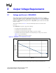
• Figure 2-1displays the load current over time.
NOTE:
1. Voltage regulator thermal protection circuitry should not trip for load currents greater than Icc
TDC
Figure 2-1. VRM/EVRD 10.1 Load Current vs. Time
100
105
110
115
120
125
0.01 0.1 1 10 100 1000
Time (s)
Load Current (A)