
Voltage Regulator Module (VRM) and Enterprise Voltage Regulator-Down (EVRD) 10.1 Design Guidelines


Voltage Regulator Module (VRM) and Enterprise Voltage 15
Regulator-Down (EVRD) 10.1 Design Guidelines
Output Voltage Requirements
The processor load may not be sufficient to absorb all of the energy from the output capacitors on
the baseboard, when VID changes to a lower output voltage. The VRM/EVRD design should
ensure that any energy transfer from the capacitors does not impair the operation of the
VRM/EVRD, the AC-DC supply, or any other parts of the system.
2.8 Overshoot at Turn-On or Turn-Off - REQUIRED
The core VRM/EVRD output voltage should remain within the load-line regulation band for the
VID setting, while the VRM/EVRD is turning on or turning off, with no over or undershoot out of
regulation. No negative voltage below –100 mV may be present at the VRM/EVRD output during
turn-on or turn-off.
2.9 Output Filter Capacitance - REQUIRED
The output filter capacitance for the VRM/EVRD based designs will be located on the baseboard.
The system design must ensure that the output voltage of the VRM/EVRD conforms to the load
line of Figure 2-2 with the baseboard and processor loads. Table 2-2 shows the number of
decoupling caps recommended and other related specifications based on updated processor power
requirements supported by VRM/EVRD 10.1.
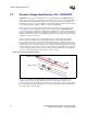
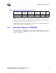
Figure 2-7. Dynamic VID Transition States Illustration
high VID to low VID
Vcc transition
450 mV
50 µs maximum settling
from registering final VID
450 mV
low VID to high VID
Vcc transition
The diagram assumes steady state, constant current during the dynamic VID
Transition for ease of illustration; actual processor behavior allows for any dIcc/dt
event during the transitions, depending on the code it is executing at that time
VID 5
36 VID steps @ 5 µs each step = 180 µs
Upper equals
Final VID-1.25mΩ*Icc
Lower equals
Start VID-1.25mΩ*Icc - 40mV
Maximum
Vcc
settling
Upper equals
Start VID-1.25mΩ∗Icc
Lower equals
Final VID-1.25mΩ*Icc - 40mV
50 µs maximum settling
from registering final VID
VID 4
VID 3
VID 2
VID 1
VID 0
400 ns
worst case VID
settling time