
ITP700 Debug Port Design Guide


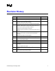


R
ITP700 Debug Port Design Guide 5
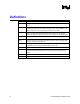
Figures
Figure 1. PWR Routing and Usage................................................................................... 13
Figure 2. Recommended Layout Topology ....................................................................... 17
Figure 3. ITP700 Flex Required Layout of Reset .............................................................. 20
Figure 4. ITP700 Flex Required Layout of BPM[5:0]#....................................................... 21
Figure 5. PWR Routing and Usage................................................................................... 25
Figure 6. TDI/TDO Scan Chain ......................................................................................... 28
Figure 7. Recommended Bypass Jumper Configuration .................................................. 29
Figure 8. Recommended Layout Topology ....................................................................... 31
Figure 9. ITP700 DPA Debug Port Pinout (Top View) ...................................................... 33
Figure 10. Debug Port Connectors.................................................................................... 41
Figure 11. Isometric View of Debug Port Adapter Keepout Volume ................................. 42
Figure 12. Front, Side, and Top View of ITP Debug Port Adapter Keepout Volume ........ 43
Figure 13. ITP LVPDA Debug Port Pinout (Top View) ...................................................... 45
Figure 14. ITP700 Flex Mechanical Drawing .................................................................... 54
Figure 15. Top View of Surface Mount ITP700 Flex Connector on the Target System .... 55
Figure 16. BPM[5:0]# Connectivity for Intel
®
Xeon™ Processor with 512-KB L2 Cache at
2.20, 2.0, and 1.80 GHz DP / Intel
®
Xeon™ Processor MP Servers ......................... 57
Figure 17 – BPM[5:0]# Connectivity for Intel
®
Pentium
®
4 Processor, Intel
®
Pentium
®
4
Processor-M, and Systems Based on Intel
®
Centrino
™
Mobile Technology .............. 60
Figure 18 – ITP Clock Routing options using System Clock Driver .................................. 62
Figure 19 – ITP Clock Routing Options Using ITPCLKOUT[1:0] Pins .............................. 63
Figure 20. Intel
®
Itanium
®
2 IO Domain BPM Connectivity................................................ 72
Figure 21. Complete Bypass of One Out of Two Agents .................................................. 77
Figure 22. Complete Bypass of Two Agents with Three Headers .................................... 77
Figure 23. Three-pin Bypass Option ................................................................................. 78
Figure 24. Illegal Bypass Configuration............................................................................. 78
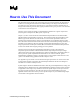
Tables
Table 1. Recommended Debug Port Signal Terminations................................................ 12
Table 2. System Signal Layout Guidelines........................................................................ 14
Table 3. JTAG Signal Layout Guidelines .......................................................................... 15
Table 4. Execution Signal Layout Guidelines .................................................................... 16
Table 5. ITP700 Flex Edge Connector Pinout................................................................... 18
Table 6. Recommended Debug Port Signal Terminations................................................ 19
Table 7. Reset Definitions ................................................................................................. 20
Table 8. BPM[5:0]# Definitions.......................................................................................... 21
Table 9. ITP700 Flex Deltas from Standard ITP AC/DC Specifications............................ 22
Table 10. Recommended Debug Port Signal Terminations.............................................. 24
Table 11. System Signal Layout Guidelines...................................................................... 26
Table 12. JTAG Signal Layout Guidelines ........................................................................ 27
Table 13. Execution Signal Layout Guidelines .................................................................. 29
Table 14. ITP700 DPA System Signal Descriptions.......................................................... 34
Table 15. JTAG Signal Descriptions ................................................................................. 35
Table 16. Execution Signal Descriptions........................................................................... 35
Table 17. ITP700 DPA System Signal DC Characteristics ............................................... 36
Table 18. ITP700 DPA JTAG Signal DC Electrical Characteristics .................................. 37
Table 19. ITP700 DPA Execution Signal DC Electrical Characteristics............................ 38