
ITP700 Debug Port Design Guide

R
28 ITP700 Debug Port Design Guide
Debug Port Signal Layout Guideline
TDI, TDO JTAG scan data signals. These signals require minor timing and signal
integrity analysis / simulation, These signals are routed point-to-point, possibly
through device bypass mechanisms. The terminations should be located within
300 ps to each load. TDI is driven on the falling edge of TCK at the ITP and
recovered on the following rising edge of TCK at the processor.
TRST# Non-critical JTAG reset signal routed to all scan chain devices. TRST#
requires a pull-down resistor to ensure the signal is held in the asserted (low)
state if the debug port is not driving the signals. Layout of this signal needs to
be such that noise will not be coupled to the signal and cause a false reset of
the scan chain.
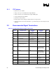
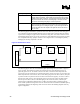
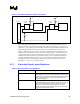
The following figure demonstrates a possible JTAG scan chain for a processor node debug port. It
is a requirement to pull up TDI/TDO between each scan chain agent. Note that when the number
of processors is changed, a bypass must be used for the empty sites. Care must be taken to ensure
that multiple pull-up resistors do not get connected to a single TDI/TDO net if bypassing of empty
sites is implemented using “jumpers”. Failure to do so might result in overloading and possibly
damaging the sourcing component or the ITP.
Figure 6. TDI/TDO Scan Chain
P1
TDI TD0
P2
TDI TD0
P3
TDI TD0
P4
TDI TD0
TD0
TDI
Chipset
TDI
TD0
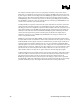
The following figure shows the recommended bypass option using a four-pin header to bypass a
device location. This method can remove devices from the scan chain whether the device is
physically present or not. To include a device in the chain, connect the TDO output from the
previous device in the chain (Pin-2) to the TDI input of the current device (Pin-1), and connect the
TDO output from the current device (Pin-3) to the TDO going to the next device (Pin-4). The pull-
up resistor needs to be placed on the current device TDI to function properly. To remove a device
from the scan chain, (device can be physically present or not present) connect the TDO output
from the previous device (Pin-2) to the TDO going to the next device (Pin-4). This four-pin
jumper bypass configuration eliminates drive conflicts encountered when a partially bypassed
device is still capable of driving data to onto the JTAG data chain. Note that the TDI/TDO pull-up
requirements defined in the beginning of this section are met in the following diagram under any
bypass configuration.