
Intel Xeon Processor Multiprocessor Platform Design Guide

98
Methodology for Determining Topology and Routing Guidelines
9.1.2.2 Hold Margin
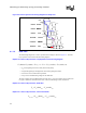
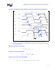
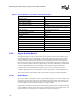
Figure 9-6 illustrates the timing diagram that was used to develop the final timing equations.
Equation 9-13. Common Clock Hold Margin
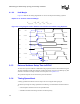
9.1.3 Data and Address Setup Time to BCLK
The Intel Xeon processor MP has an additional timing requirement for the data and address signals.
The data and address signals must meet the specified setup time to the processor BCLK[1:0]. This
should be calculated as a simple common clock setup time as in Equation 9-12.
The specified setup time can be found in the processor datasheet.
9.1.4 Timing Spreadsheet
A timing spreadsheet should be created to keep track of each signal's timing margins.
To effectively manage the timing spreadsheet the following recommendations should be adhered
to.
• All assumptions should be stated in the spreadsheet file
• Simulated and measured timings should be tracked separately
Figure 9-6. Timing Diagram Used to Determine the Common Clock Hold Timing Equations
holdskewholdpropdrvholdinm
TTTTT
__arg
−−+=
CLK Out A
CLK Out B
CLK In
A
B
A
B
CLK
CLK
CLK
CLK
CLK
DATA
DATA
T
drv
T
prop
T
hold
T
prop_clk
(A)
T
prop_clk
(B)
T
drv_clk
(B)
T
drv_clk
(A)
T
margin_hold