
Intel Xeon Processor Multiprocessor Platform Design Guide

35
System Bus Routing
6.3.2 Chipset System Bus I/O Decoupling Recommendations
The primary objective of the I/O decoupling recommendations for the chipset is to provide clean
power delivery to the system bus I/O buffers. The split power-plane nature of chipsets creates this
power delivery concern. A noisy or starved power supply will negatively impact the signal quality
and/or drive strength seen on the system bus signals.
The secondary objective of decoupling at the chipset is to minimize the impact of return path
discontinuities that may occur between the chipset package and the motherboard. A return path
discontinuity occurs in systems whose signals reference either power or ground, but not both. The
chipset uses symmetric stripline interconnects that reference the signal to both V
CC_CPU
and V
SS
.
Systems that have this type of discontinuity should use the larger number of decoupling capacitors
listed in the below guidelines for the chipset.
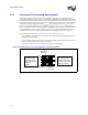
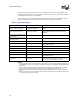
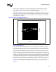
The decoupling recommendations for the chipset are (shown in Figure 6-3):
• Four minimum, five preferred 0.1 µF capacitors with 603 packages distributed evenly over the
system bus data lines
• Two minimum, three preferred 0.1 µF capacitors with 603 packages distributed evenly over
the system bus address and common clock lines
• All capacitors placed as close to the chipset package as the chipset keep-out zone allows.
Double-sided platforms should place the caps on the backside close to the V
CC_CPU
and V
SS
pins of the system bus.
6.4 Routing Guidelines for a 4-Way System
This section provides more details for 4-way processor systems. This information is subject to
change. Both recommendations and considerations are presented.
For proper operation of the Intel Xeon processor MP and Intel Xeon processor MP with up to
2-MB L3 cache on the 0.13 micron process system bus it is necessary to meet the timing and
voltage specifications of each component on the bus. The most accurate way to understand the
signal integrity and timing of the system bus on the platform is by performing a comprehensive
simulation analysis. It is conceivable that adjustments to trace impedance, line length, termination
impedance, board stack-up and other parameters can be made that improve system performance.
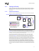
Figure 6-3. System Bus I/O Decoupling Guidelines for the Chipset
Address and
Cntrl Field
Data Field
Example
Chipset
Package
6-9 0.1[ uF ] with 603 body
over the data signals and as
close to the chipset package
as possible
4-5 0.1[ uF ] with 603 body
over the data signals and as
close to the chipset package
as possible
4-6 0.1[ uF ] with 603 body
over the address and cntrl
signals and as close to the
chipset package as possible
2-3 0.1[ uF ] with 603 body
over the address and cntrl
signals and as close to the
chipset package as possible