
Intel Xeon Processor and Intel E7500/E7501Chipset Compatible Platform Design Guide

Intel
®
Xeon™ Processor and Intel
®
E7500/E7501 Chipset Compatible Platform Design Guide 225
Schematic Checklist
Schematic Checklist 13
13.1 Processor Schematic Checklist
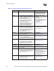
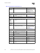
Table 13-1. Processor Schematic Checklist (Sheet 1 of 4)
Checklist Items Recommendations Comments
A20M#
IGNNE#
INIT#
LINT0/INTR
LINT1/NMI
SMI#
SLP#
STPCLK#
• Connect to both processors and Intel
®
ICH3-
S. Include 200
Ω ± 5% pull-up to VCC_CPU.
• Asynchronous GTL+ Input Signal.
• Refer to Section 5.3.6.
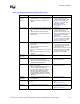
A[35:3]#
1
ADSTB[1:0]#
2
D[63:0]#
3
DBI[3:0]#
DSTBN[3:0]#
4
DSTBP[3:0]#
5
REQ[4:0]#
6
• Connect to both processors and the MCH. • AGTL+ Source Synchronous I/O.
• Refer to Section 5.1.
ADS#
AP[1:0]#
DBSY#
DP[3:0]#
DRDY#
LOCK#
BPRI#
DEFER#
RS[2:0]#
RSP#
TRDY#
8
• Connect to both processors and the MCH. • AGTL+ Common Clock I/O.
• AGTL+ Common Clock Input
• Refer to Section 5.2.
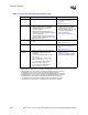
FERR#/PBE#
IERR#
PROCHOT#
THERMTRIP#
• If supported, connect to both processors and
the ICH3-S. Terminate at both ends with
56
Ω ± 5% pull-up to VCC_CPU.
• If not supported, leave as no-connect or
connect to a Baseboard Management
Controller (BMC).
• Asynchronous GTL+ Output.
• Refer to Section 5.3.2.
BINIT#
BNR#
HIT#
HITM#
MCERR#
• Connect to both processors and the MCH.
• Route as common clock signal.
• AGTL+ Common Clock I/O
Wired-OR signals.
• Refer to Section 5.2.1.
BCLK[1:0] • Connect to a 49.9
Ω 1% pull-down and to a
series resistor (20 – 33
Ω). Connect other
side of series resistor to CK408.
• System Bus Clock.
• Refer to Section 4.1.
NOTE: BCLK[1:0] are processor pin
names that are connected to clocks in
the Host_CLK clock group on
CK408B.