
Intel Xeon Processor and Intel E7500/E7501Chipset Compatible Platform Design Guide

Platform Power Delivery Guidelines
186 Intel
®
Xeon™ Processor and Intel
®
E7500/E7501 Chipset Compatible Platform Design Guide
11.2.6 Voltage Sequencing
When designing a system with multiple voltages, there is always the issue of ensuring that no
damage occurs to the system during voltage sequencing. Voltage sequencing is the timing
relationship between two or more voltages such as VCC_CPU and SM_VCC/VID_VCC.
SM_VCC/VID_VCC is defined as 3.3 V for the processor.
The processor’s BSEL[1:0] outputs use an active driver. A 3.3 V source connected to the
processor’s 3.3 V pins supplies the VID output. The BSEL[1:0] outputs will be valid within 1 ms
after the 3.3 V supply reaches 95% of its nominal value. The system logic must ensure that the
clock driver device (e.g., CK408) does not use these inputs until after the BSEL[1:0] signals are
valid. An example implementation could utilize the CK408’s VTT_PWRGD_N input signal by
keeping it deasserted until BSEL is valid. Depending on the design of the system's power
sequencing logic, the PWR_OK signal from the power supply may be used to drive this CK408
input signal. Or, this signal could be driven by existing power sequencing delay logic that monitors
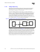
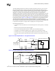
the 3.3 V supply. See Figure 11-10 for an example of this implementation.
A voltage of 3.3 V is required for correct operation of the processor VID logic. The processor’s
VID outputs use an active driver. As shown in Figure 11-11, the VID outputs will be valid within
1 ms after the 3.3 V supply reaches 95% of its nominal value. The system power supply should
generate PWR_OK no less than 100 ms after all of its outputs reach their respective 95% values.
PWR_OK may be used to enable the VR output. For example a supply adhering to ATX12V design
guidelines meets this requirement. The VR’s PWRGD output may be used to generate the
PWRGOOD input to the processor. PWR_OK should be deasserted when any output of the supply
falls below 95% of its nominal value (also consistent with ATX12V). It is important to maintain
SM_VCC anytime the output of the VR is enabled. Driving the VR’s OUTEN control input with
the PWR_OK signal will ensure correct sequencing at both power-up and power-down.
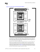
Figure 11-10. CK408 / Processor Power Sequencing Requirement
2N3904
+V3_3
BSEL0
+V3_3
Pow e r
Supply
PWROK
1 kΩ
10 kΩ
3.3V
Processor
CK408
VDD
S1
VTT_PWRGD_N