
VRM 9.1 DC-DC Converter Design Guidelines
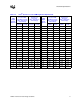
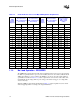
Table Of Contents
- 1 Electrical Specifications
- 1.1 Output Requirements
- 1.1.1 Voltage and Current - REQUIRED
- 1.1.2 Maximum Ratings - EXPECTED
- 1.1.3 Output Voltage Tolerance - REQUIRED
- 1.1.4 No-Load Operation - REQUIRED
- 1.1.5 Turn-on Response Time - EXPECTED
- 1.1.6 Overshoot and Undershoot at Turn-On or Turn-Off - REQUIRED
- 1.1.7 Converter Stability - REQUIRED
- 1.1.8 Current Sharing - REQUIRED
- 1.2 Input Voltage and Current
- 1.3 Control Inputs - REQUIRED
- 1.4 Remote Sense (VO-sen+, VO-sen-) - EXPECTED
- 1.5 Power Good Output (PWRGD) - REQUIRED
- 1.6 VRM Present (VRM-pres) - EXPECTED
- 1.7 Efficiency - PROPOSED
- 1.8 Isolation - PROPOSED
- 1.9 Fault Protection
- 1.1 Output Requirements
- 2 Module Layout Guidelines
- 3 Environmental Conditions
- 3.1 Operating Temperature - PROPOSED
- 3.2 VRM Board Temperature - REQUIRED
- 3.3 Non-Operating Temperature - PROPOSED
- 3.4 Humidity - PROPOSED
- 3.5 Altitude - PROPOSED
- 3.6 Electrostatic Discharge - PROPOSED
- 3.7 Shock and Vibration - PROPOSED
- 3.8 Electromagnetic Compatibility - PROPOSED
- 3.9 Reliability - PROPOSED
- 3.10 Safety - PROPOSED

VRM 9.1 DC-DC Converter Design Guidelines 13
Electrical Specifications
1.1.5 Turn-on Response Time - EXPECTED
The output voltage should reach its specified range within 15 ms after the input power reaches its
minimum voltage and the OUTEN signal is asserted.
1.1.6 Overshoot and Undershoot at Turn-On or Turn-Off
- REQUIRED
Overshoot must be less than 2% above the Voltage Identification (VID) code. No negative voltage
below −0.1 V may be present at the output at any time.
1.1.7 Converter Stability - REQUIRED
The VRM, operating independently or paralleled with other VRMs, needs to be unconditionally
stable under all output voltage ranges and current transients with system board capacitance ranging
from 5,000 µF to 20,000 µF and with less than 2.0 mΩ ESR.
1.1.8 Current Sharing - REQUIRED
Multi-processor applications require that current-sharing capability be available to avoid power-
plane splits.
One pin of the VRM is reserved for control of star-point or single-wire current sharing. This pin
will be connected to other VRMs within the system. VRMs designed for current sharing by means
of accurate output control need not use this pin. If a VRM does not use the current share pin, the
pin should not be connected on the module.
There is no time limit for response to power-up or transients: VRMs must meet all other electrical
specifications during transitions, and output current levels must not damage the VRMs.
1.1.8.1 Current Sharing Tolerance - REQUIRED
The output current of any VRM should match the output current of all paralleled VRMs within
10% of the rated output current over the full output current range, except during initial power-up.
For instance, if a particular VRM model is designed to supply a 50 A processor as a maximum, the
difference between the output currents of two or more VRMs in parallel may be as much as 5 A at
any value of current actually produced, even to the point where one VRM is producing 5 A, and
one in parallel with it is producing no current in supplying a 5 A load.
The VRM must supply current equal to the total load multiplied by the ratio of (1 + tol) and
(n + tol) where “tol” is the current sharing accuracy and “n” is the number of VRMs sharing the
load. Current sharing accuracy better than 10% would allows the VRM to be designed for a lower
output current. It may more cost effective to design to a looser current sharing accuracy and a
higher output current. For example, assuming a 300 A load supplied by four parallel VRMs, each
would need to be designed for 77.8 A and 80.5 A for respective current share accuracies of 5% and
10%.
1.1.8.2 Interoperability Between Manufacturers - EXPECTED
Current sharing among different VRM models, including VRMs from different manufacturers, is
an expected feature. However, cost optimization and difficulties involved with fully testing
interoperability may preclude use of this feature.